Hersteller von Keramiksubstraten
Keramische Substrate verfügen über hervorragende elektrische Isolationseigenschaften und werden häufig in der Elektronik und Elektrik eingesetzt. Anwendung: Industrie, erneuerbare Energien und Fahrzeugelektrifizierung
Bestes Preis-Leistungsverhältnis!
Kundenspezifische Lieferung von Keramiksubstraten
In modernen elektronischen Systemen werden vor allem Keramiksubstrate verwendet. GORGEOUS bietet kundenspezifische Lösungen mit Keramiksubstraten wie Aluminiumoxid, Aluminiumnitrid, Zirkoniumoxid, Siliziumnitrid und Siliziumkarbid.
Wir bieten alle gängigen Keramiksubstrate auf dem Markt aus einer Hand. Neben Keramiksubstraten bieten wir auch Dünnschichtschaltungsfertigung, Laserbearbeitung und metallisierte Substrate an und fertigen so hochwertige Dünnschichtkeramiksubstrate und Keramiksubstrat-Leiterplatten. Kontaktieren Sie uns, um die optimale Lösung für Ihre Anforderungen zu finden.
Anpassbares Keramiksubstratmaterial
Verschiedene Materialien zur Auswahl!
Wir geben Ihnen die besten Materialempfehlungen basierend auf Ihren Anwendungsanforderungen und fertigen die am besten geeigneten Keramiksubstrate, Dickschichtkeramik-Leiterplatten usw. individuell an.
Aluminiumoxidsubstrat
Das am häufigsten verwendete Keramiksubstrat in der Industrie, im Bereich erneuerbare Energien, der Automobilelektrifizierung und der Hochleistungselektronik. Individuell anpassbar. Senden Sie uns eine Nachricht, um ein Angebot zu erhalten.
AlN-Substrat
AlN zeichnet sich durch eine hohe Wärmeleitfähigkeit und einen Wärmeausdehnungskoeffizienten (CTE) aus, der dem von Silizium sehr nahe kommt. Daher wird es hauptsächlich in der Eisenbahn, in der Industrie, im Bereich erneuerbarer Energien und in LEDs eingesetzt. Kundenspezifische Anpassungen sind möglich. Senden Sie eine Nachricht, um ein Angebot zu erhalten.
Zirkonoxidsubstrat
Es verfügt über eine hohe Biegefestigkeit und Bruchzähigkeit und eignet sich daher ideal für Heizungs-, Sensor- und Automobilanwendungen. Anpassungen sind möglich. Bitte senden Sie eine Nachricht, um eine Anfrage zu erhalten.
Siliziumnitridsubstrat
Hohe Biegefestigkeit, hohe Bruchzähigkeit und gute Wärmeleitfähigkeit machen es für Elektrofahrzeuge und industrielle Anwendungen geeignet. Senden Sie eine Nachricht, um eine Anfrage zu erhalten.
Berylliumoxid-Substrat
Es verfügt über eine außergewöhnlich hohe Wärmeleitfähigkeit und Wärmeableitungsfähigkeit und unser Unternehmen ist in der Lage, es sicher und konform zu verarbeiten. Senden Sie uns eine Nachricht, um ein Angebot zu erhalten.
SiC-Substrat/Wafer
Dank der extrem hohen Wärmeleitfähigkeit und der hervorragenden mechanischen Eigenschaften eignet es sich ideal für Leistungselektronik, 5G-Basisstationen und HF-Geräte, LEDs und mehr. Senden Sie uns eine Nachricht, um ein Angebot zu erhalten.
Direkt verbundenes Kupfer
Direct bonded copper (DBC) is primarily used in power semiconductors, semiconductor refrigeration, UPS uninterruptible power supplies, photovoltaics, and other applications.
Reactive Metal Brazing Substrates(AMB)
Reactive metal brazing substrates are used in fields such as high-speed trains, new energy vehicles, high-voltage power grids, and communications.
Standardgröße des Substrats
| Substratgröße (mm) | Maßabweichung (mm) |
| 50.8*50.8 | ±0,2 |
| 76.2*76.2 | ±0,3 |
| 101.6*101.6 | ±0,4 |
Substratdicke
Die Substratdicke beträgt 0,1–3 mm, mit typischen Dicken von 0,254, 0,381, 0,508 und 0,635. Die Substratdickentoleranz beträgt ±10%.
| Dicke (mm) | Dickentoleranz (mm) | ||
| Wie gefeuert | Boden | Poliert | |
| 0.127 | ±0,012 | ±0,005 | ±0,005 |
| 0.254 | ±0,025 | ±0,005 | ±0,005 |
| 0.381 | ±0,038 | ±0,005 | ±0,005 |
| 0.508 | ±0,050 | ±0,01 | ±0,01 |
| 0.635 | ±0,063 | ±0,01 | ±0,01 |
| 0.762 | ±0,076 | ±0,01 | ±0,01 |
| 1.016 | ±0,10 | ±0,01 | ±0,01 |
Technische Möglichkeiten
| Substrattyp | Oberflächenrauheit | Verzug |
| Wie gefeuert |
Vorne: ≤100 nm Rückseite: ≤200nm |
0.3% |
| Boden | Nach Kundenwunsch | 0.1% |
| Poliert | ≤25 nm | 0.1% |
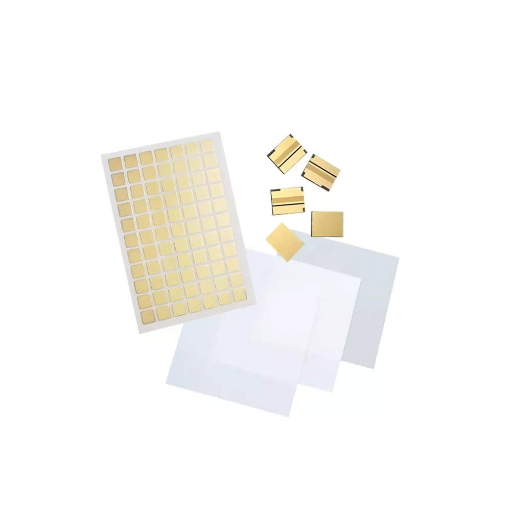
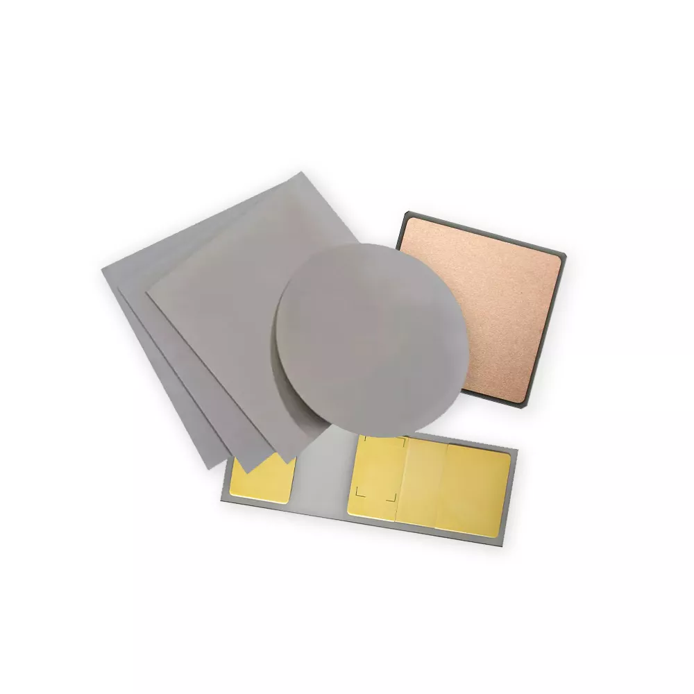
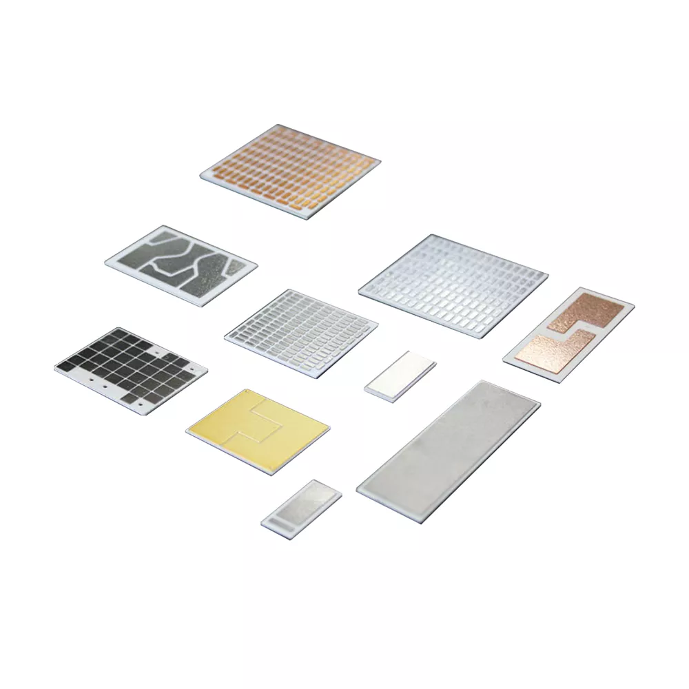
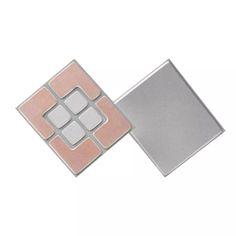
Laser und metallisierte Substrate
Bei GORGEOUS bieten wir eine flexible Auswahl an fortschrittlichen Fertigungsverfahren, darunter Hartbearbeitungstechnologien wie Stanzen, Laserbearbeitung und Trockenpressen, die auf die Bedürfnisse unserer Kunden zugeschnitten sind, basierend auf Anwendungsszenarien, Materialeigenschaften, Geometrie und Produktionslosgrößen.
Wir bieten hochpräzise Metallisierungen für die Keramiksubstrate unserer Kunden, sodass diese direkt mit elektronischen Bauteilen bestückt werden können. Unsere proprietäre Metallisierungslotpaste bietet hervorragende Haftung und Fließfähigkeit und gewährleistet so einen stabilen und zuverlässigen Lötprozess.
Während des Metallisierungsprozesses bildet sich auf der Oberfläche unserer Substrate eine gleichmäßige leitfähige Schicht. Diese sorgt nicht nur für einen effizienten Leiterpfad und zuverlässige elektrische Verbindungen für elektronische Komponenten, sondern verhindert auch wirksam, dass Korrosion und andere Umwelteinflüsse die Leistung des Substrats beeinträchtigen.


Dünnschicht-Schaltkreisverarbeitung
GORGEOUS fertigt Dünnschichtschaltungen für unsere Kunden. Unsere automatisierte Produktionslinie für Dünnschichtschaltungen bietet Komplettlösungen für hybride integrierte Dünnschichtschaltungen, die Materialien, Design, Herstellung und Anwendung umfassen.
Die Anwendungsmöglichkeiten für diese integrierten Dünnschicht-Hybridschaltungen sind vielfältig und umfassen Leistungsteiler, Koppler, Mikrowellen-/Millimeterwellenfilter, Mikrowellen-/Millimeterwellen-Dämpfungsglieder, Ferritzirkulatoren, Mikrowellen-/Millimeterwellengeräte, Laserdiodengehäuse, hochdichte Verbindungen und D/AA/D-Wandler.
Wenn Sie Dünnschicht-Keramiksubstrate, Keramiksubstrat-Leiterplatten oder metallisierte Keramiksubstrate benötigen, kontaktieren Sie uns bitte umgehend und wir bieten Ihnen den besten maßgeschneiderten Service!
Häufig gestellte Fragen
Welche keramischen Substratmaterialien bietet GORGEOUS an?
Wir bieten Substrate aus Aluminiumoxid, Aluminiumnitrid, Siliziumnitrid, Berylliumoxid und Siliziumkarbid an. Darüber hinaus bieten wir metallisierte Keramiksubstrate und die Verarbeitung von Dünnschichtschaltungen an.
Was sind die Unterschiede zwischen Al2O3-, AlN- und Si3N4-Substraten?
Aluminiumoxid bietet Kosteneffizienz und gute Isoliereigenschaften; Aluminiumnitrid bietet eine ausgezeichnete Wärmeleitfähigkeit und Siliziumnitrid bietet eine hohe mechanische Festigkeit, gute Wärmeleitfähigkeit und gute Isoliereigenschaften.
Für welche Anwendungen werden Keramiksubstrate verwendet?
Keramische Substrate werden vor allem in Elektrofahrzeugen, erneuerbaren Energien, der Industrie, der Luftfahrttechnik, der Leistungselektronik und anderen Bereichen eingesetzt.
Welche Metallverbindungstechnologien unterstützen wir?
Wir unterstützen AMB (Active Metal Brazing), DCB (Direct Copper Bonding) und SMB (Sputtered Metal Bonding).