Ceramic substrates or sheets are used in various industries due to their high thermal conductivity, high electrical insulation, corrosion resistance, and high wear resistance. Substrates are an essential part of the latest developments. This is because they offer basic support and are crucial components of electric circuits.
Continue reading this blog till the end to know more about the main ceramic substrates, how they replace metals in 3C electronic devices, their applications, and their advantages.
The 3 most common ceramic substrates are aluminum oxide, aluminum nitride, and beryllium oxide.
1 Aluminum Oxide (Al2O3) ceramic substrate: It is one of the most popular ceramic substrates. The surface of aluminum oxide is smooth and has low porosity. It is used in industrial, renewable, and vehicle electrification. They are used to manufacture biomedical implants, high-temperature furnace tubes, and catalytic converters.
2 Aluminum Nitride (AlN) ceramic substrate: It offers high mechanical strength, resistance to chemical products, high thermal conductivity, high resistance to wear and corrosion, and high electric insulation. They are mainly used in sintering equipment, oven construction elements, medical technology, and electronic sensors.
3 Beryllium Oxide (BeO) ceramic substrate: This is the best thermal conductor and electric insulator. Its electric insulation is similar to that of Alumina. It is usually used in the manufacturing of electronic insulators and substrates which require effective heat dissipation to maintain device performance and stability. They are used in microwave devices, vacuum tubes, magnetrons, and gas lasers.
Why Choose Ceramic Substrates?
Ceramic Substrate has excellent properties that make it suitable for use in electronic devices. Ceramics are proven to be better than metals due to their excellent thermal, mechanical, and chemical qualities. Below mentioned are some of its major properties:
1 Physical Properties: Its physical properties are best for portable devices since they require lightweight material for manufacturing. The substrate material reduces the net weight of the device.
2 Chemical Properties: The organic substrate can bear high temperature and is corrosion and oxidation-resistant. It is also best for use in electrical devices due to its insulation properties.
3 Mechanical Properties: Ceramic material offers high wear resistance that allows long-lasting performance, as you read before. This makes them perfect for high-performance computing, and 5G communication equipment.
Metal substrates have always been utilized in 3C electronics because of their conductivity and toughness. But, problems like ineffective heat dissipation, corrosion risk, and the weight of metal substrates are appearing as technology advances. These flaws affect the working and durability of modern electronic equipment.
Therefore, to overcome these challenges ceramics are now being used and proven to be effective in 3C electronics.
Applications of Ceramic Substrates in 3C Electronics
There are many applications of ceramic substrates. A few of them are as follows:
1 Consumer Electronics: Ceramic Substrates are popularly being used in consumer electronics. It is used in smartphones to reduce the thickness of the device and heat management. Ceramic substrates offer durability and lightweight making them suitable for wearable devices.
2 Computer Devices: The main function of ceramic substrates is to dissipate heat for continuous performance. Laptops and tablets require durability and portability which is offered by ceramics.
3 Communication Devices: Ceramic substrates have become an essential component of the base station modules, antennas, and power amplifiers. This is mainly due to the advancement of the 5G network.
Advantages of Ceramic Substrates
There are many advantages of ceramic substrates. Some of them are listed below:
1 Sustainable: Ceramic substrates improve portability due to their light-weight further reducing the weight of the device. Ceramics are environmentally friendly as compared to metals. It also supports green production techniques.
2 Environment Adaptability: Ceramics are known to tolerate harsh environments such as high temperature, high humidity, and corrosive conditions. Electronic devices last longer due to ceramic’s flexibility. It further requires less maintenance and repairs.
3 Performance Improvements: Ceramics helps in improving the overall performance. It efficiently dissipates the heat and reduces the risk of overheating. This makes them perfect to use in high-frequency communication applications that provide regular and reliable performance.
Uses of Ceramics in ICs and Semiconductors
IC (Integrated Circuits) Packaging
ICs are made up of interconnected silicon chip components. Ceramic packages are used to provide electrical insulation and hermetic support in integrated circuits.
Semiconductor
The main ceramic in the semiconductor sector is fused silica. Fused silica is used in crucibles for silicon ingots, reactors for epitaxial silicon deposition, wafer carriers, single-wafer processing tools, and wet etch tanks.
Alumina is also used in semiconductor wafer processing equipment. This is due to its electrical and thermal insulation properties. It provides low dielectric constant and loss, high thermal conductivity, and chemical stability required for the performance and reliability of IC substrates and the manufacturing of ceramic semiconductor materials.
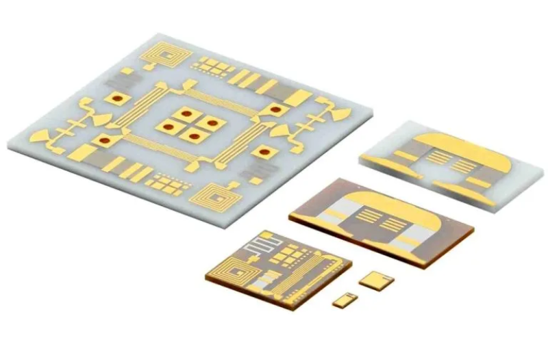
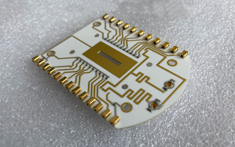
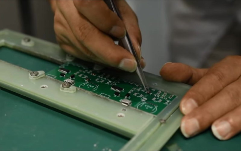
Ceramic PCBs

Ceramics are great insulators that prevent the flow of electric current. They are popularly used in high-frequency electronics, LED lighting, and power electronics. This is generally because it dissipates heat to improve performance and longevity. It is also used as a substrate material in Printed Circuit Boards (PCBs). Ceramic PCBs are mainly used in applications that require little CTE (Coefficient of Thermal Expansion) and circuits that require high thermal conductivity.
The Ceramic Printed Circuit Boards are also used in power electronics to manage high temperatures and provide the thermal stability required for proper heat dissipation. Ceramic circuit boards are flexible and durable. Therefore, they can be customized to create complex mechanical and electrical designs.
FR-4 (Flame Retardant-4) is widely recognized as a standard material for the production of PCBs. It is an epoxy resin laminate material reinforced with glass which is used as a ceramic pcb material. The normal fr4 cte is 14 to 17 ppm/°C.
You must know how to measure the pipes. This will help you to choose the ones you need and fulfill your requirements. There are various ways in which you can measure the pipes. Some of these are listed below:
1 Outer Diameter (OD): You can measure the outer diameter of the pipes. Simply take the measurements from one external outline of the pipe to its opposite outline. The distance between the two points will give you the outer diameter. Outer diameter also includes the thickness of the pipe.
2 Inside Diameter (ID): You must measure the inside diameter of the pipes. This provides you with the volume of the pipe and exactly tells you how much of the substance can it hold. To do this, measure the one end of the internal outline of the pipe to its opposite outline. Now, the distance between the two points will be the internal diameter. Internal diameter does not include the thickness of the pipe.
3 Nominal Pipe Size (NPS): NPS tells you the general size of the pipe. You can understand it by adding the internal diameter with half the thickness of the pipe. This will result in the nominal size of the pipe. For instance, if the NPS of a pipe is 4, then the outer diameter will be 4.5 inches and not 4 inches.
Dimensions of OD, ID, and NPS
It is important to understand the dimensions of the outer diameter, inside diameter, and nominal pipe size to measure the pipes accurately. The dimensions are as follows:
Outer Diameter (OD): If you want to measure the outer diameter of a 1-inch pipe, you would be surprised to know that it would measure 1.342 inches and not 1 inch. This is because of the obvious reason that it also includes the thickness of the material.
Internal Diameter (ID): In the case of internal diameter it will be smaller than the outer diameter as it does not include the thickness of the pipe. For example, if a 2-inch Schedule 40 pipe has an outer diameter of 2.375 inches then its internal diameter would be 2.067 inches.
People generally look for internal diameter for the selection of PVC pipes. This is because it will give the correct size that you need. Considering the outer diameter can give you a bigger size of the PVC pipe than required.
Nominal Pipe Size (NPS): The value of NPS is generally smaller than the outer diameter. If the value of the nominal pipe size is 2 inches then the outer diameter will be 2.375 inches. It is a standard set of pipe sizes made in North America.
Thickness of Pipe Walls
The pipe walls come in various thicknesses. It is known as Schedules. The most popular thickness of pipes is 40. You can use Schedule 80 to use pipes with greater thickness and strength. This shows that thicker walls will make the pipe stronger and long-lasting.
Conclusion
After reading this blog you must have gained enough knowledge about the three ceramics substrates that have subsequently replaced metals in 3C electronic devices. It offers various advantages such as sustainability, environment adaptability, and performance improvements. Ceramic substrates are also used in integrated circuits and semiconductors.