With 2D materials getting popular in electronic and optoelectronic applications, the search for an efficient substrate resulted in exploring HBN. As the conventional substrates posed implications on the quality of 2DM grown, HBN proved to be better alternative. Let us check on what makes Hexagonal Boron Nitride a better substrate?
What is Boron Nitride (BN)? Is Boron Nitride a Compound?
Knowing Boron Nitride (BN) chemistry is equally important before advancing to learn it’s properties. Boron Nitride is a chemical compound which is crystalline in nature made up of Boron and Nitrogen. Boron Nitride formula is “BN”. The BN molecule is isoelectronic to carbon i.e. it exhibits similar structure and electronic configuration but differs in element placements.
Boron Nitride (BN) Structure
Knowing the structural specialty of Boron Nitride helps us to explain the functionality of the HBN better.
Majorly, Boron Nitride structure is of Three types: Amorphous, Hexagonal, Cubic and Wurtzite.
-
Amorphous Boron Nitride – ABN structure
Amorphous form of Boron Nitride is disoriented and is equivalent to Carbon. They do not possess regularity on how the atoms are arranged or in short terms has no structural configuration. Other than ABN, all other forms of Boron Nitride follow crystalline structure.
-
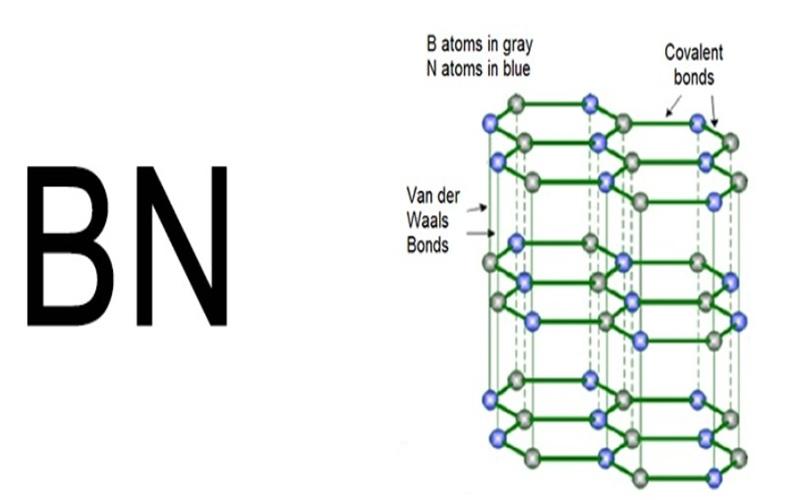
Hexagonal Boron Nitride - HBN Structure
HBN, known as white graphene is considered to be extremely stable with layered structure. The layers in the structure are held together by Vander Waals force of attraction. The BN compound present in each layer is bonded to the layer through by Covalent bonds. Have a look at the structure of Hexagonal Boron Nitride given below.
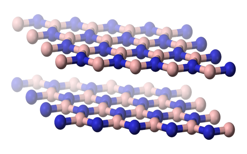
Coming to the monolayer of HBN, the monolayer of Hexagonal Boron Nitride is quite similar to Graphene. It follows a honeycomb structure with similar dimensions. Unlike graphene they are not black but white in appearance. HBN as a material function as better electrical insulators.
-
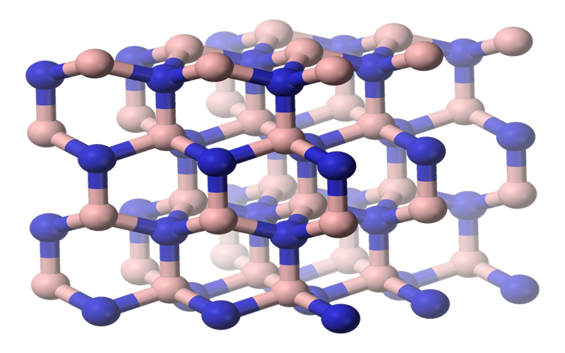
Cubic Boron Nitride – CBN Structure
In terms of stability cubic boron Nitride tends to be less stable than that of HBN. However, the conversion rate between the structures at room temperature is comparatively negligible. A reference image showing the structure of CBN is given below. The sphalerite structure of Cubic Boron Nitride is analogous to diamond
-
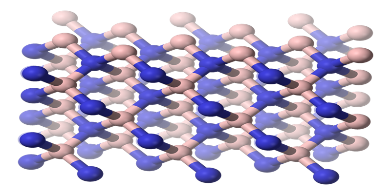
Wurtzite Boron Nitride -WBN structure
WBN follows a boat configuration where the BN compound forms a 6 membered ring as given in the image. The structure of Wurtzite boron Nitride is analogous to the polymorph of Carbon known as Lonsdalaite. The hardness of Wurtzite Boron nitride is estimated to be in the range of 46 GPa.
Properties of Boron Nitride: A quick glance
The below tabulation summarizes the Important properties of Boron Nitride pertaining to different structure: Amorphous, Wurtzite, Cubic and Hexagonal.
|
Properties |
ABN |
HBN |
WBN |
CBN |
|
Boron Nitride density (g/cm3) |
2.3 |
2.1 |
3.5 |
3.5 |
|
Boron Nitride Thermal Conductivity (W/Mk) |
3 |
600 (II layer) 30 (I layer) |
740 |
|
|
Band Gap (Ev) |
5 |
6- 6.4 |
4.5 – 5.5 |
10-10.7 |
|
Refractive Index of Boron Nitride |
1.7 |
1.8 |
2.1 |
2 |
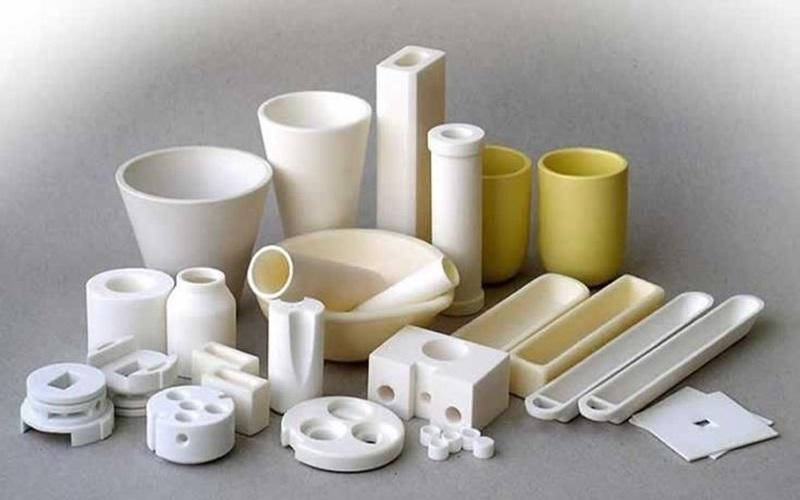
What are advanced Ceramics? Whether HBN is one among them?
Before getting into the specialties of HBN as an advanced ceramic, let us learn more on what is advanced ceramic. Advanced Ceramics as the name suggests are superior new generation ceramics that have competitive properties over traditional ceramic. They are thermally stable, possesses superior electrical resistance, are chemically inert and has higher thermal conductivity similar to metals. Some of the popular Advanced Ceramic materials are given below:
Alumina
Alumina is a widely used advanced ceramic made up of Aluminium Oxide. The ionic inter atomic bonds present in alumina structure makes them extremely stable. They are good electrical insulators. Alumina ceramic offers good wear and tear resistance and are mechanically strong. They are used in lithium-ion batteries, pump materials, spark plugs, sensors in automobiles and electrical insulation.
Silicon Carbide (SiC)
Silicon Carbide Sic is formed through sintering of Carbide grains. The Ceramic is known for its extreme hardness. Naturally, SiC is found in moissanite. Silicon carbide is popularly used in power electrics due to their strong endurance to high voltages. The hardness of the ceramic makes it suitable to function as Car brakes, armors and automobile clutches.
Zirconia Ceramic
Zirconia ceramic exhibits good fracture toughness in comparison with all the other ceramics. Zirconia is of different grades when stabilized such as Yttria or magnesia stabilized Zirconia or partially stabilized Zirconia. They are often utilized in dental Ceramics and are generally used in combination with metals.
Silicon Nitride
Silicon Nitride is said to be resistant to oxidation and impactful thermal gradients. They are used in variety of structural applications. The properties of SiC makes it useful to be an engine component. They are used to produce cutting tools and the biocompatibility makes them useful as dental and medical implants.
Boron Nitride (BN) as an Advanced Ceramic
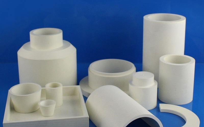
Boron Nitride, is considered as a machinable an advanced ceramic. They offer good thermal conductivity, lubricity, Higher di-electrical strength and lesser dielectric constant. Boron Nitride is also known as White graphene due to the structural similarity it has with graphene. They are good electrical insulators and also resists higher oxidation temperature.
As discussed earlier, Boron Nitride tends to exist in different structural Configurations. The properties of the popular types of BN are given below:
-
Cubic Boron Nitride
Cubic Boron Nitride has hardness around 4500 Kg per mm2 which is comparable to diamond. It is manufactured by high temperature and Pressure compression of Hexagonal Boron Nitride. The thermal stability, thermal Conductivity and electrical resistivity of Cubic Boron Nitride are considered to be on higher side.
When used along with alloys of Nickel, Iron or any other compounds Cubic Boron Nitride tend to stay inert. The extreme hardness of Cubic Boron Nitride makes them function as better grinding tools. They are also used in Automobiles as engine parts, heat sink for electronic equipments and are good electrical insulators.
-
Hexagonal Boron Nitride (HBN)
Knowing the properties of HBN as an advanced ceramic is very important before using it in applications. H Boron Nitride is a stable ceramic which has a single 2D layer similar to graphene. They are thermally stable up to an air temperature of 1000 degC and stands even higher under vacuum conditions. They are chemically inert in nature and can stand acids but degrades in molten salts and alkaline compounds.
The nanoribbons of HBN holds a thermal conductivity range of 1700 W/mK to 2000 W/mK. They are often used as substrates, battery materials and are quite common in thermal applications
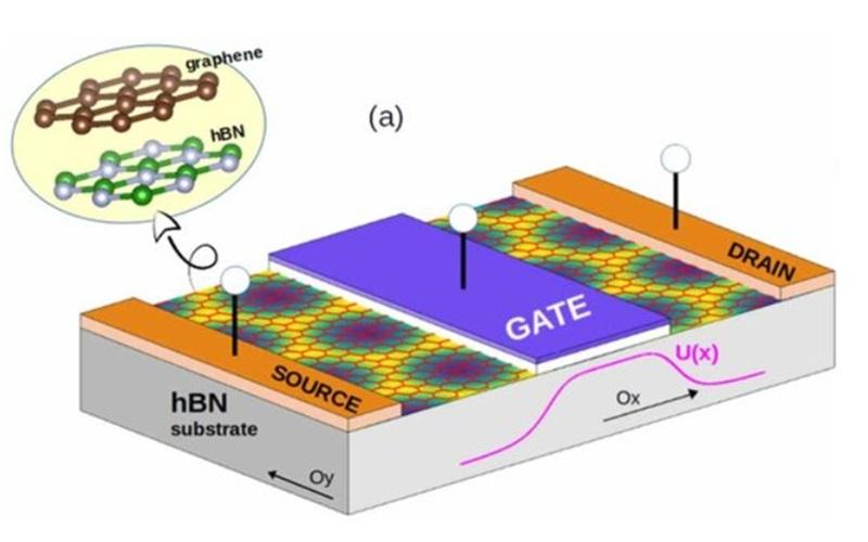
HBN as ideal Substrate for 2D Materials
The recent advancement has hailed HBN being a perfect substrate for 2D materials. Before proceeding further, let us explore what are 2D materials?
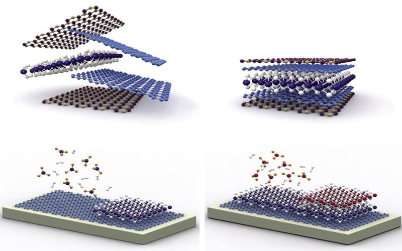
2D materials are single layered materials existing in nanoscale. They are manufactures by techniques such as chemical vapor deposition or Mechanical and Liquid Exfoliation. The Specialties of single layered materials (2DM) include the following:
-
2DM has Higher tensile strength.
-
2DM offer higher area to volume ratio which helps chemical reactants to have increased contact time.
-
They have Supreme optical, mechanical and electrical properties
HBN as an Ideal substrate for 2D materials
The popular manufacturing technique used to prepare 2D materials is Chemical Vapor Deposition (CVD). The process uses a heated chamber where the reaction happens at controlled pressure, temperature and fixed time. The atoms under the process conditions hits on the substrate to form 2D materials on top of it. The modern material science prefers HBN as a 2DM substrate in Photonic and Electronic devices due to merits listed below.
General Merits of HBN
Hexagonal Boron Nitride has evident advantages over Conventional SiO2/Si substrates. The thermal stability at elevated temperatures, the resistance to oxidation and corrosion are the major take aways. The single layer structure of HBN with BN compound bonded by covalent bonds can be manipulated which aids CVD process. The structural stability of Hexagonal Boron Nitride is another Key factor.
Morphological Merits of HBN
The 2D materials synthesized on Conventional SiO2/Si are inferior and are majorly disordered. The architecture and functionality get compromised when the substrate turns inefficient. Hexagonal Boron Nitride on the other hand offers a smooth flat atomic surface with no charge traps contrary to other substates. The lattice constant of HBN is similar to Graphene which merits the 2DM synthesis of graphene devices.
The defect density of Hexagonal Boron Nitride is comparatively less. The Vander walls forces present in HBN layers also ensures the growth of 2DM that has any property mismatch with HBN. Some of the known outcomes of using HBN include the development of superior graphene 2DM with high mobility. With HBN as a substrate, a controlled growth of 2DM is observed that increases efficiency of devices.
Conclusion
The functionality of H Boron Nitride is overwhelming when compared to conventional substrates. The atomic structure similarity with materials such as graphene has resulted in synthesizing competitive 2DM’s. HBN with its weak force between layers enable production of variety of 2D materials which makes them a modern substrate of merit.