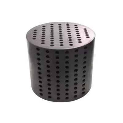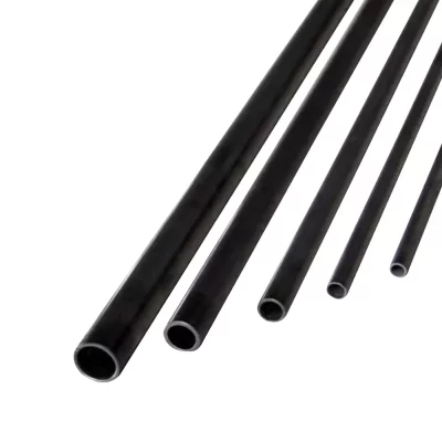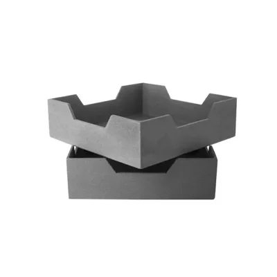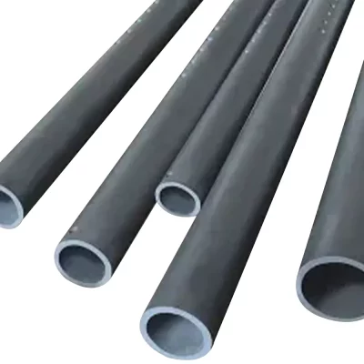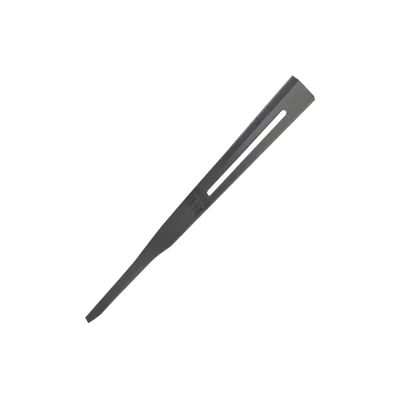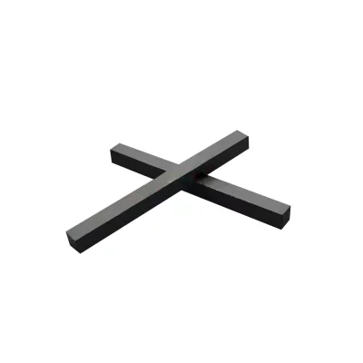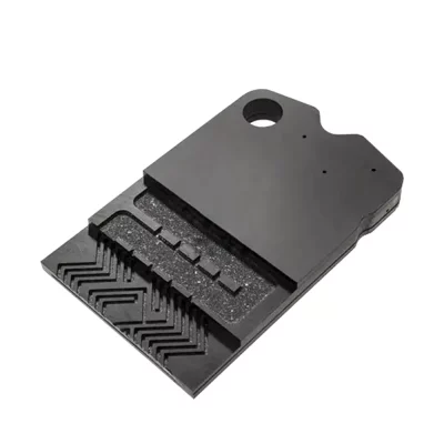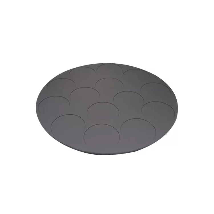
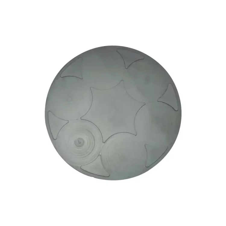
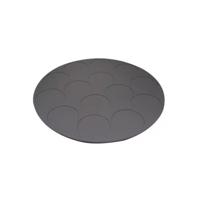
GORGEOUS CERAMICS (GGS Ceramic) silicon carbide PVD carriers are manufactured using isostatic pressing and high-temperature sintering processes. We can precisely machine the carrier’s outer diameter, thickness, number and size of cavities, as well as the position and shape of the pick-up slots, according to the user’s design drawings to meet your application requirements.
Delivery Time
We customize products according to customer drawings (custom sampling), and the delivery time is generally 3-4 weeks.
For standard products in stock, we ship quickly within 24-48 hours.
For your urgent products, we can provide you with a green channel for expedited production.
Paket
- Our products are packaged with dual protection against static electricity and moisture: the inner layer uses a high-quality anti-static/moisture-proof vacuum bag.
- Custom-designed cushioning and shock-absorbing clips secure the product: We use dust-free, high-density, molded suspended clips to secure the product, ensuring 360° protection against impacts and vibrations during transportation.
Advantages of silicon carbide PVD carriers
Anti-plasma erosion
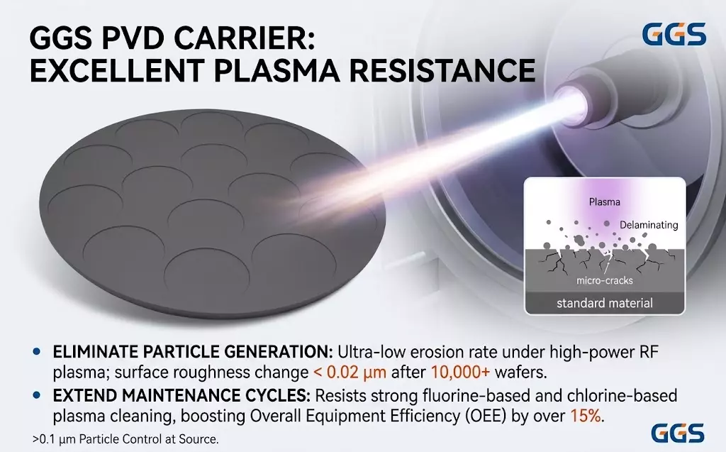
GORGEOUS CERAMICS (GGS Ceramic) PVD carriers are specifically designed for high-density plasma and physical vapor deposition environments.
Under prolonged bombardment by high-energy RF plasma, ordinary materials are prone to developing micron-level microcracks and spalling. GORGEOUS CERAMICS (GGS Ceramic) silicon carbide materials, with their high density and zero-porosity structure, achieve extremely low gas etching rates, and after continuous bombardment testing with over 10,000 wafers, the surface roughness change is less than 0.02 μm.
Reducing particulate matter at the source: The product surface is free of dust shedding, effectively controlling particulate matter production to >0.1 μm, reducing the probability of wafer edge contamination.
Extended maintenance intervals: The product can withstand strong fluorine/chlorine-based plasma cleaning, improving the overall efficiency of the equipment by more than 15%.
Ultimate thermal uniformity
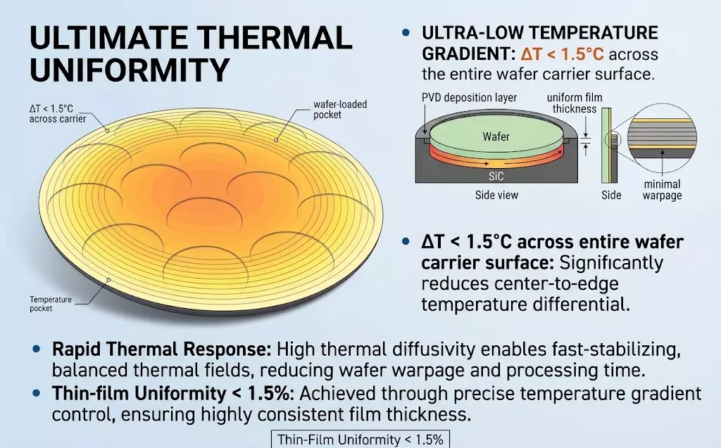
During PVD thin film deposition, minute gradient changes in the thermal field on the carrier surface directly cause differences in deposition rates, leading to uneven film thickness between the wafer edges and center.
GORGEOUS CERAMICS (GGS Ceramic)’s silicon carbide PVD carriers possess high thermal conductivity and an ultra-low coefficient of thermal expansion. Compared to traditional materials, they significantly reduce the temperature difference ΔT between the center and edge of the carrier surface to < 1.5°C.
- Eliminating thermal stress and thermal hysteresis: The product’s high thermal diffusivity enables rapid thermal response, quickly establishing a balanced thermal field during heating and cooling cycles, reducing wafer deformation caused by thermal stress.
- Ensuring film thickness uniformity: GGS Ceramic maintains a highly consistent deposition rate for PVD metal/dielectric films by controlling the temperature gradient across the entire wafer within an extremely narrow range, significantly improving film uniformity to < 1.5%.
High-frequency thermal cycling makes it less prone to cracking

PVD processes frequently subject the process chamber to high-frequency thermal cycles of preheating, deposition, rapid cooling, and in-situ cleaning. The peak thermal stress generated within the carrier disk is a major cause of microcracks, thermal deformation, and even failure.
To address this issue, GORGEOUS CERAMICS (GGS Ceramic) silicon carbide PVD carrier disks, with their extremely low coefficient of thermal expansion, high fracture toughness, and high thermal conductivity, can rapidly release accumulated thermal stress even under drastic heating/cooling rates and high-frequency thermal cycling, significantly reducing the risk of thermal fatigue cracking and micro-scraping.
- Resistant to thermal fatigue: Withstands over 50,000 extreme thermal cycling tests, maintaining product structural integrity without microcrack propagation.
- Excellent dimensional stability: Deformation <5μm under long-term high-frequency cycling, preventing wafer misalignment or vacuum adsorption failure due to carrier disk warping.
Silicon Carbide PVD Carrier Disk Product Specifications
|
Außendurchmesser |
Toleranz |
Dicke |
Toleranz |
Chip size and number of chips |
|
230 |
±0.1 |
3 |
±0.05 |
4 inches, 3 pieces |
|
300 |
±0.1 |
1.4 |
±0.05 |
4 inches, 5 pieces |
|
300 |
±0.1 |
3 |
±0.05 |
4 inches, 5 pieces |
|
300 |
±0.1 |
1.4 |
±0.05 |
4-inch (7 pieces), 6-inch (2 pieces) |
|
300 |
±0.1 |
3 |
±0.05 |
4-inch (7 pieces), 6-inch (2 pieces) |
Häufig gestellte Fragen
What are the main advantages of silicon carbide PVD substrates?
Silicon carbide PVD substrates offer excellent resistance to plasma attack, high thermal conductivity, and thermal stability.
These superior properties ensure uniform temperature distribution during deposition, effectively reducing particulate contamination and extending the substrate’s lifespan in the PVD process environment.
Why is temperature uniformity crucial in Physical Vapor Deposition (PVD) processes?
In Physical Vapor Deposition (PVD) processes, temperature uniformity directly affects film thickness consistency and coating quality. GGS’s silicon carbide substrates provide rapid and uniform heat transfer, thereby improving PVD film deposition yield.
How does silicon carbide perform under rapid heating and cooling cycles?
Silicon carbide exhibits strong thermal shock resistance, capable of withstanding frequent rapid heating and cooling without cracking or deformation.
Which silicon carbide fabrication process do you use?
We offer high-density modified reactive sintering and pressureless sintering (SSiC) substrates, with various processes available to meet your process requirements.
How to regenerate and clean a substrate if a thick layer of metal waste (such as Ti, Ta, Cu, Ag) has been deposited on the substrate surface?
Silicon carbide has extremely strong resistance to acid and alkali corrosion. You can use strong acids to strip away the accumulated metal deposits on the surface without damaging the physical dimensions and surface roughness of the SiC substrate itself.