Cerámica semiconductora
Desde el procesamiento de obleas, la adsorción al vacío y el ensamblaje de precisión hasta los procesos de alta temperatura, GORGEOUS ofrece a los clientes soluciones integrales de cerámica semiconductora personalizadas.


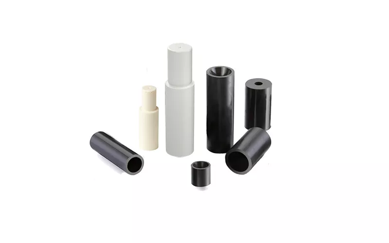


Piezas estructurales de cerámica de precisión
Industria de pan-semiconductores
Descripción de la cerámica semiconductora
La cerámica avanzada es una parte fundamental de los equipos de fabricación de semiconductores. Durante la fabricación de semiconductores se genera una gran cantidad de plasma, por lo que es crucial utilizar materiales resistentes al plasma como componentes de equipos. En comparación con los metales, las resinas y el vidrio, las cerámicas avanzadas ofrecen mayor rendimiento y fiabilidad. Su resistividad suele estar entre conductores y aislantes, y su excelente aislamiento eléctrico las hace muy adecuadas para la fabricación de semiconductores.
Te proporcionamos todos los materiales cerámicos que necesitas:
✅Alúmina (Al2O3) — Ultraalta pureza y rigidez;
✅Nitruro de aluminio (AlN) — Excelente conductividad térmica y aislamiento;
✅Nitruro de silicio (Si3N4) — Tenacidad a la fractura ultra alta y bajo coeficiente de expansión térmica;
✅Carburo de silicio (SiSiC)— Baja densidad y coeficiente de expansión térmica.
De acuerdo a sus necesidades, ¡podemos recomendarle el mejor material para crear componentes cerámicos semiconductores de ultra alta precisión!
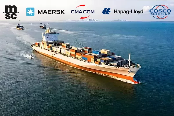
Garantía de tiempo de fabricación y envío
¡GORGEOUS coopera con varias empresas internacionales líderes de logística para producir para usted rápidamente y entregarle los productos a tiempo e intactos!
La fabricación y el transporte de cerámica se ven afectados por el proceso y su ubicación. Fabricaremos rápidamente para usted según su plan y elegiremos el mejor método de transporte. Entrega aérea más rápida en América del Norte, llega en 7 días.
Las empresas de logística con las que cooperamos incluyen:
- MSC (Compañía Naviera del Mediterráneo)
- Maersk
- CMA CGM
- COSCO
- Hapag-Lloyd
- DHL
- Unión Postal Universal
- FedEx
- TNT
Trabajamos con múltiples transportistas para garantizarle opciones de envío eficientes a precios más bajos, entrega a tiempo, y ¡Sin cargos ocultos!

Fabricación

Embalaje

Cargando
Transporte
Propiedades principales de la cerámica semiconductora

Alta dureza

Resistente al desgaste

Resistente a la corrosión

Resistencia a altas temperaturas

Aislamiento fuerte
PRECIOSA Referencia de Precisión de Producto Personalizable
| Tecnología de procesamiento | parámetro | Precisión alcanzable |
| Molienda | Planitud, paralelismo, Ra | Ra≥0,05 μm” Planitud <1 μm |
| Molienda | Llanura | 5 μm < Ø 200 mm / 10 μm > Ø 200 mm |
| Aspereza | Ra de 0,15 μm a 0,6 μm | |
| Paralelismo | 5 μm < Ø 200 mm / 10 μm > Ø 200 mm | |
| Erosionando | Simétrico | Máx. 0,05 mm (orificio/ranura de posicionamiento) |
| Pulido | Planitud, paralelismo, rugosidad | Ra0,06 μm-0,35 μm Planitud <2 μm Paralelismo<2μm |
| Estructuración | Aspereza | Rugosidad < 3,2 μm Tamaño < 150 μm |
*La precisión específica debe determinarse de acuerdo con el material, la forma y los requisitos del proceso del producto real.

Proceso opcional de cerámica semiconductora
| Tipo de producto | Solicitudes especiales |
| Sustrato cerámico | Pulido, recubrimiento metalizado, chapado en oro. |
| Brazo de cerámica | Pulido de espejo, ranuras de ventilación, revestimiento antiestático. |
| Anillos/juntas de cerámica | Chorro de arena, recubrimiento de teflón, recubrimiento de superficies |
| Tubo de cerámica | Pulido de paredes interiores, prensado isostático en caliente, recubrimiento de superficies. |
| Ventosa de cerámica | Procesamiento de microagujeros, procesamiento de agujeros ciegos, diseño de ventilación de adsorción |
| Elemento calefactor cerámico | Recubrimiento metalizado, esmalte de superficie, recubrimiento antiestático. |


Parámetros y selección de materiales cerámicos semiconductores personalizados

| Artículo | Unidad | Nitruro de silicio |
| Densidad | g/cm3 | >3.2 |
| Dureza | – | HRA90 |
| Dureza Vickers (Hv50) | HV0.5 | >1550 |
| Módulo de elasticidad | GPa | 290 |
| Resistencia a la flexión | MPa | >600 |
| Resistencia a la compresión | MPa | 2500 |
| Tenacidad a la fractura | MPam1/2 | >6.0 |
| Temperatura máxima de uso | °C | 1200 |
| Conductividad térmica | W /(M·K) | 15-20 |
| Coeficiente de expansión térmica | 10-6 /°C | >3.1 |
| Resistencia al choque térmico | △T℃ | 500 |
| Capacidad calorífica específica | KJ/kg·K | 700 |
| Rigidez dieléctrica | KV/mm | 1 |
| Constante dieléctrica | εr | – |
| Resistividad volumétrica a 20℃ | Ω.cm | 1.0×10¹² |
| Artículo | Unidad | Carburo de silicio sinterizado sin presión | Carburo de silicio unido por reacción | Carburo de silicio sinterizado recristalizado |
| Temperatura máxima de funcionamiento | °C | 1600 | 1380 | 1650 |
| Densidad | g/cm3 | >3.1 | >3.02 | >2.6 |
| Porosidad | % | <0.1 | <0.1 | 15% |
| Resistencia a la flexión | MPa | >400 | 250 (20 °C) | 90-100 (20 °C) |
| MPa | – | 280 (1200 ℃) | 100-120 (1100 ℃) | |
| Módulo elástico | GPa | 420 | 330 (20 °C) | 240 |
| GPa | – | 300 (1200 ℃) | – | |
| Conductividad térmica | W/mk | 74 | 45 (1200 ℃) | 24 |
| Coeficiente de expansión térmica | K-1×10⁻⁶ | 4.1 | 4.5 | 4.8 |
| Dureza Vickers | GPa | 22 | 20 | – |
| Resistencia a ácidos y álcalis | – | excelente | excelente | excelente |
| Propiedad | Unidad | Alabama2Oh3 99.7 | Alabama2Oh3 99.5 | Alabama2Oh3 99 | Alabama2Oh3 95 |
| Pureza | — | 99.7% | 99.5% | 99% | 95% |
| Densidad | g/cm3 | 3.92 | 3.9 | 3.8 | 3.7 |
| Resistencia a la flexión | MPa | 375 | 370 | 340 | 304 |
| Resistencia a la compresión | MPa | 2450 | 2300 | 2250 | 1910 |
| Módulo elástico | GPa | 380 | 370 | 330 | 330 |
| Tenacidad a la fractura | MPam1/2 | 4.5 | 4.3 | 4.2 | 3.8 |
| Dureza | HRA | 91 | 91 | 90 | 89 |
| Dureza Vickers | HV1 | 1600 | 1550 | 1450 | 1400 |
| Coeficiente de expansión térmica | 10- 6 K-1 | 7.8 | 7.8 | 7.7 | 7.5 |
| Conductividad térmica | W/mk | 32 | 32 | 25 | 25 |
| Estabilidad al choque térmico | △T.℃ | 220 | 220 | 200 | 200 |
| Temperatura máxima de funcionamiento | °C | 1750 | 1750 | 1700 | 1500 |
| Resistencia de volumen a 20℃ | Ω·cm | 1015 | 1015 | 1014 | 1014 |
| Rigidez dieléctrica | KV/mm | 22 | 20 | 16 | 15 |
| Constante dieléctrica (temperatura ambiente) | / | 10 | 11 | 11.5 | 11 |
| Factor de pérdida dieléctrica de MHz | tan δ | 1×10⁻³ | 1×10⁻³ | 3×10⁻³ | 3×10⁻³ |
| Artículo | Unidad | Nitruro de aluminio |
| Densidad | g/cm3 | 3.31 |
| Módulo de elasticidad | GPa | 310 |
| Tenacidad a la fractura | MPa × m1/2 | 3.5 |
| coeficiente de Poisson | – | 0.25 |
| Compresivo | MPa | 2100 |
| Resistencia a la flexión | MPa | 335 |
| Dureza (Vickers) | GPa | 11 |
| Dureza (Knoop 100g) | Kilogramos/mm2 | 1170 |
Referencia de tipo de extremo de eje cerámico personalizable

Productos de material de alúmina
❇️Placas de pulido de obleas:La alta dureza y resistencia al desgaste garantizan una alta precisión y una larga vida útil del pulido de obleas.
❇️Efectores finales / Manejo de obleas:Excelente resistencia mecánica y estabilidad química, adecuado para la manipulación de obleas en entornos de alta limpieza.
❇️Productos metalizados:Buena conductividad eléctrica y resistencia a altas temperaturas, adecuado para dispositivos electrónicos de alta potencia.
❇️Anillos de cámara / objetivos de pulverización catódica:La alta pureza y la resistencia a la corrosión garantizan la estabilidad y la consistencia del proceso de deposición de película delgada.
Productos de material de carburo de silicio
❇️Placas de pulido de obleas:Dureza y conductividad térmica extremadamente altas, adecuadas para un pulido de obleas eficiente y de alta precisión.
❇️Mandriles electrostáticos:La excelente conductividad térmica y el aislamiento eléctrico garantizan una adsorción estable de obleas a altas temperaturas.
❇️Mandriles de vacío:Alta resistencia y resistencia al calor, adecuado para la fijación de obleas en entornos de alto vacío.
❇️Efectores finales / Manejo de obleas:Ligero y muy rígido, adecuado para la manipulación de obleas a alta velocidad y alta precisión.
❇️Anillos de cámara:Excelente resistencia a altas temperaturas y corrosión, adecuado para entornos de procesos de semiconductores hostiles.
¿Cuáles son los usos de la cerámica semiconductora?
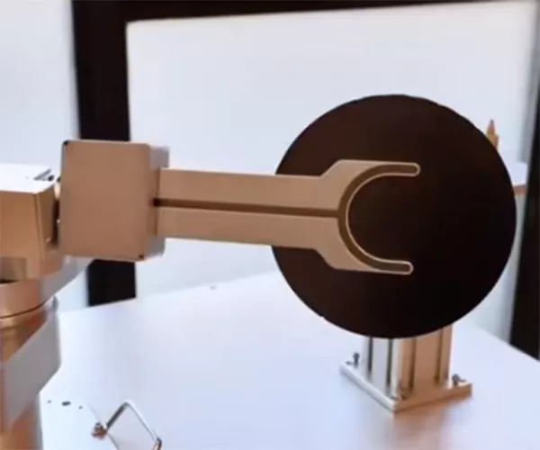
Brazo robótico de cerámica/procesador final de cerámica
El brazo cerámico desempeña la función de transporte en equipos semiconductores, equivalente al brazo de un robot. Se encarga principalmente de transportar obleas y chips de silicio a las ubicaciones designadas.

Calentador de cerámica semiconductor
Los calentadores para semiconductores poseen una excelente conductividad térmica, resistencia a altas temperaturas y aislamiento eléctrico. Se calientan de forma rápida y uniforme, y se utilizan ampliamente en la fabricación de semiconductores, equipos optoelectrónicos y otros ámbitos.

Mandril cerámico para obleas de vacío
El mandril de vacío para obleas es un dispositivo importante para el mecanizado de precisión y la fabricación de semiconductores, diseñado para fijar y manipular obleas de silicio u otros materiales delgados. Utiliza el principio de adsorción al vacío para garantizar la estabilidad de la oblea y su estabilidad durante el procesamiento, las pruebas y la limpieza.

Piezas de equipos semiconductores
Muchos dispositivos semiconductores utilizan productos cerámicos avanzados, como discos aislantes cerámicos, anillos aislantes cerámicos, termistores, cerámicas sensibles a los gases, cerámicas fotosensibles, etc.
Servicio integral de fabricación de cerámica de semiconductores
15+ Años de experiencia. Alta precisión y diseño OEM. Equipo profesional de I+D. Precio competitivo.
Nuestros éxitos con el pase Testimonios

¿Cuál es la vida útil de sus productos?
Nuestros productos cerámicos semiconductores tienen una excelente durabilidad y pueden funcionar de manera estable durante mucho tiempo en entornos de alta temperatura, alta presión y corrosivos, lo que reduce sus costos de reemplazo.
¿Cómo elegir los materiales?
Según los diferentes escenarios de aplicación, le recomendamos elegir el material adecuado:
- Nitruro de aluminio (AlN): Tiene excelente conductividad térmica (>170 W/m·K) y aislamiento eléctrico, y es adecuado para dispositivos semiconductores de alta potencia.
- Óxido de aluminio (Al₂O₃): Tiene buena resistencia mecánica y resistencia a la corrosión y es ampliamente utilizado en componentes electrónicos convencionales.
- Nitruro de silicio (Si₃N₄): tiene estabilidad a altas temperaturas y resistencia al impacto, y es particularmente adecuado para componentes clave en entornos hostiles.
Sus capacidades de personalización
Ofrecemos personalización de diversas especificaciones y estructuras complejas. Ya sea para procesamiento con precisión micrométrica o para la fabricación de piezas con formas especiales, podemos satisfacer sus necesidades.