SiC Wafers / SiC Substrates
GORGEOUS is a leading international ceramic supplier, specializing in providing customers with SIC substrates/wafer products used in new energy electric vehicles and semiconductor manufacturing. We can customize exclusive solutions based on the application!
Silicon Carbide Substrate Solutions
- Multi-Specification Wafer Supply: We offer standard wafer sizes, including 2-inch, 4-inch, and 6-inch, and can customize wafers based on customer needs.
- High-Purity Crystal Growth: We utilize advanced PVT (Physical Vapor Transport) and high-temperature sintering processes to ensure low defect density and high uniformity.
- 정밀 가공: We offer wafer dicing, grinding, polishing, and epitaxial (Epi) growth processes to ensure surface quality and flatness.
- Metallization and Post-Processing: We offer coating, ion implantation, patterning, and etching services tailored to customer needs to enhance device integration.
- Strict Testing: We conduct defect inspection, thickness uniformity testing, and surface roughness testing on every wafer to ensure it meets the diverse needs of our customers’ high-end applications.
Leading International SiC Substrate Supplier
GORGEOUS has over 15 years of expertise in high-performance ceramic substrate manufacturing, dedicated to providing customers with high-quality SiC substrates and wafers.
We utilize advanced crystal growth technology, employing high-temperature PVT, to produce large-scale, low-defect SiC crystals to meet global market demands.
We offer a complete processing chain, from crystal growth → wafer slicing → polishing → epitaxy → metallization, providing customers with a one-stop solution and ensuring consistent quality.
Our products are marketed globally and have earned the trust of numerous international customers. Whether you’re in the new energy vehicle, renewable energy, communications, or high-end semiconductor industries, GORGEOUS can meet your needs!
When you choose GORGEOUS, you’re not just choosing a supplier; you’re choosing a trusted manufacturing partner capable of large-scale production and fast delivery.
Silicon Carbide Substrate/Silicon Carbide Wafer Product Gallery
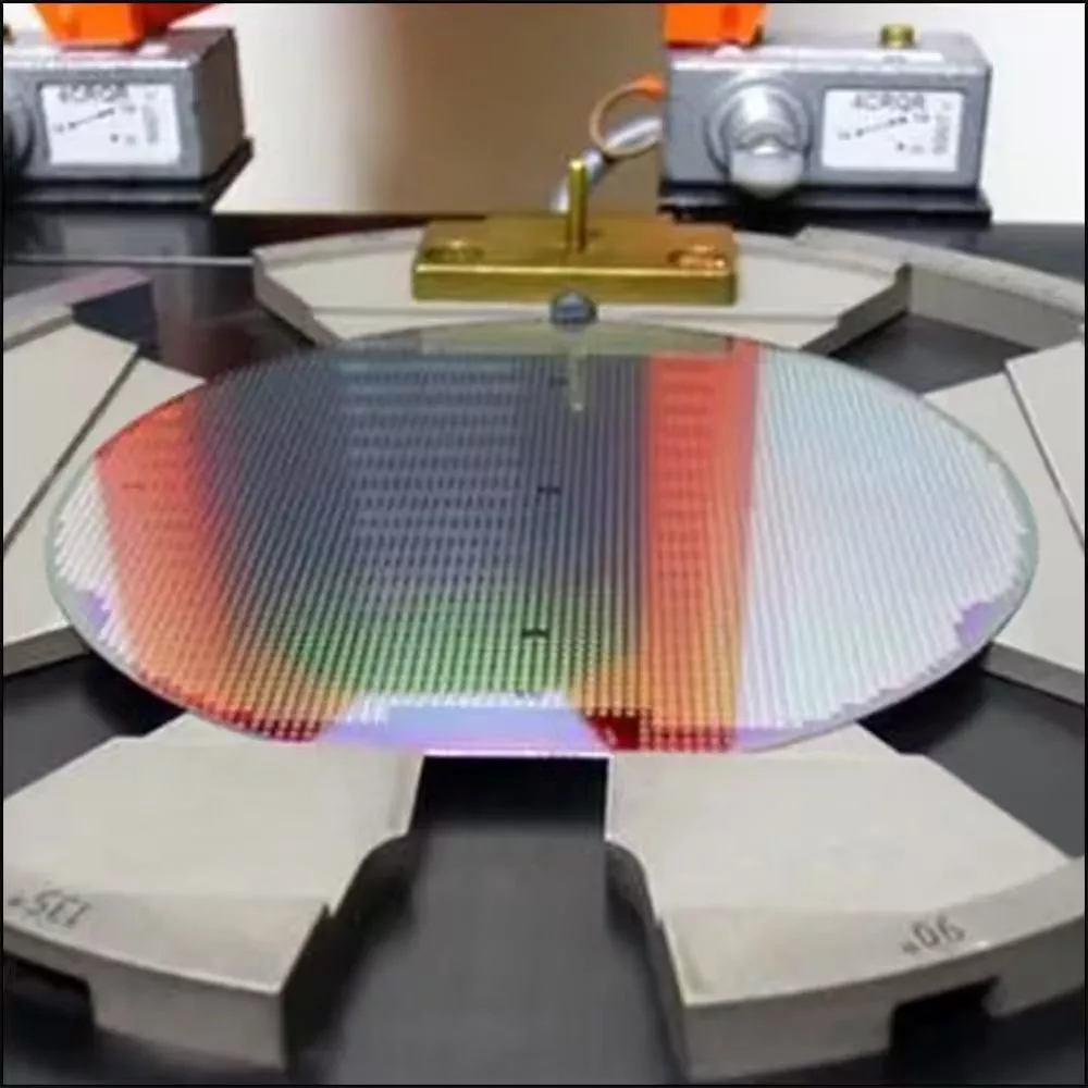
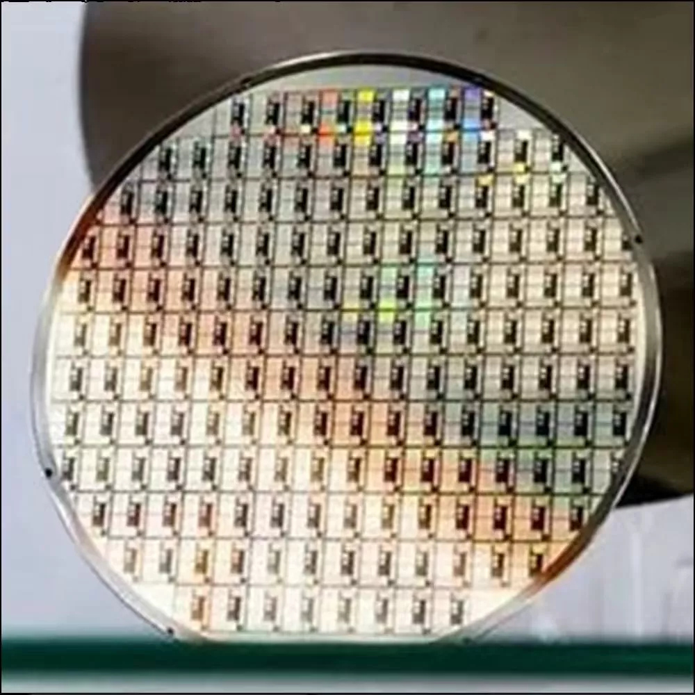
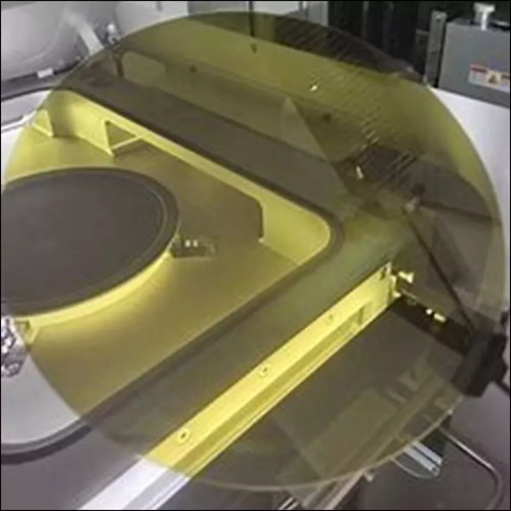
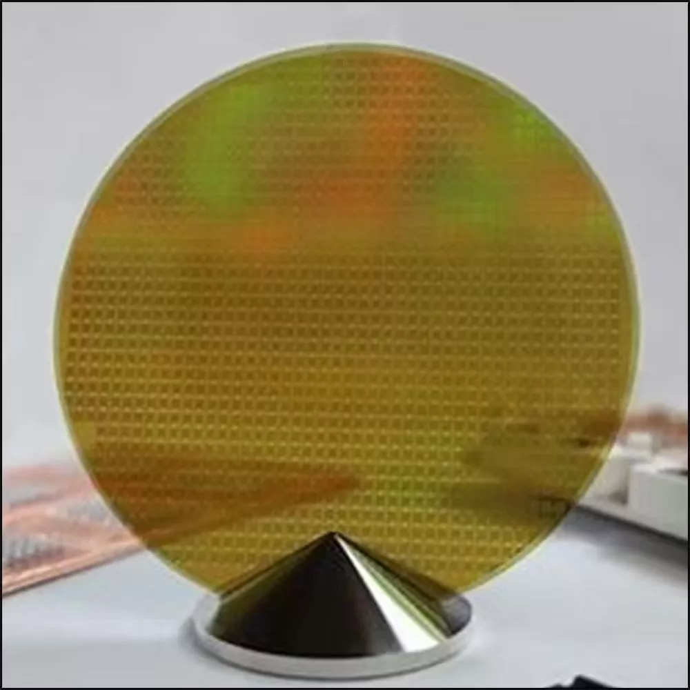
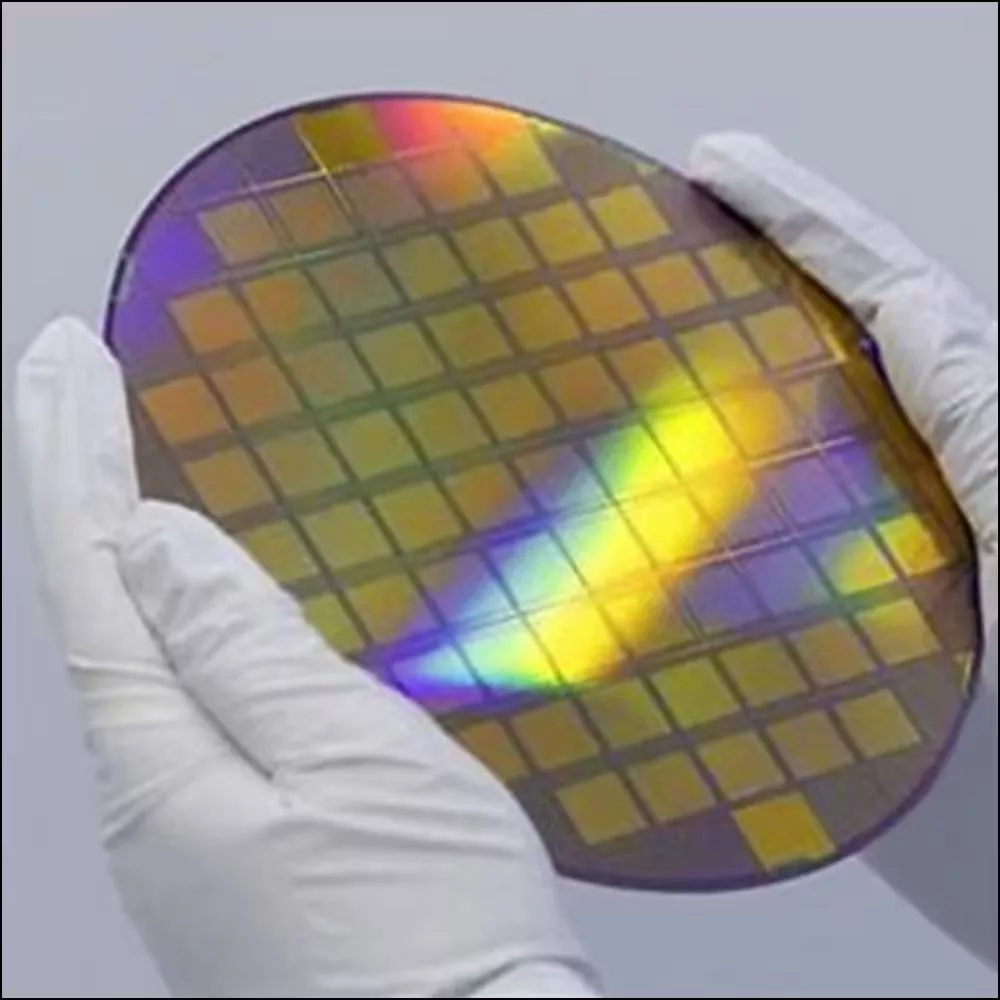
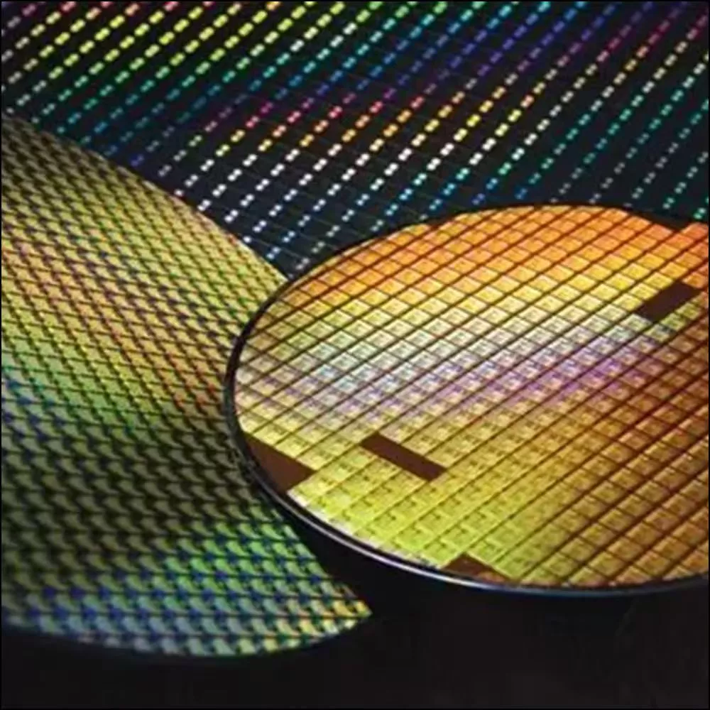
4H n-Type SiC Substrate
| Polytype | 4H |
| Diameter(mm) | 150/200 |
| Orientation(°) | 4 |
| Thickness(μm) | 350/500 |
| 표면 마감 | Epi-ready |
4H Semi-Insulating
| Polytype | 4H |
| Diameter(mm) | 100 & 150 |
| Orientation(°) | 0 |
| Thickness(μm) | 500 |
| 표면 마감 | Epi-ready |
Y
Silicon Carbide Substrate/Wafer Applications

Electronics and Semiconductor Fields
알루미나 기판은 우수한 전기 절연성 및 방열 특성을 제공하며, 인쇄 회로 기판(PCB) 및 하이브리드 집적 회로(HIC)에 활용될 수 있습니다.
전자 및 반도체 분야에서 이러한 기판의 대표적인 응용 분야로는 반도체 패키징 기판, 두꺼운/얇은 박막 회로 기판, 센서 캐리어 등이 있습니다.
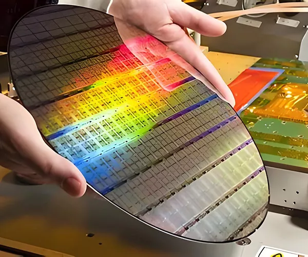
통신 및 무선 주파수(RF) 분야
알루미나 기판은 통신 및 무선 주파수(RF) 분야에서 RF 회로 기판 및 마이크로웨이브 소자 기판으로 활용될 수 있습니다. 고주파 통신(5G 기지국 및 레이더 시스템 등)에서 낮은 유전 손실과 안정적인 신호 품질을 유지합니다. 또한 마이크로웨이브 소자 기판으로서 필터, 전력 증폭기(PA), 커플러 등의 부품에 주로 사용되어 뛰어난 고주파 특성을 보장합니다.

자동차 및 신재생 에너지
알루미나 기판은 자동차 및 신에너지 차량에서 IGBT 모듈, 모터 드라이브 모듈과 같은 파워 모듈의 방열용으로 사용되어 시스템의 효율적이고 안정적인 작동을 보장합니다. 또한 차량용 전자 회로 기판으로도 활용될 수 있습니다.

조명 및 디스플레이
Alumina substrates can be used in high-power LED lamp beads to dissipate heat, helping to avoid light decay; while in laser diodes and displays, ceramic substrates can provide good electrical insulation and thermal management.

Aerospace and Military
Radar and satellite electronic devices require high-frequency, high-power, and highly reliable components, and alumina substrates can provide high insulation and thermal stability.
최소주문수량이 걱정되시나요?
Our SiC substrates offer custom monolithic manufacturing to meet small order needs. Experience our services today.
왜 GORGEOUS를 선택해야 할까요?
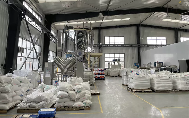
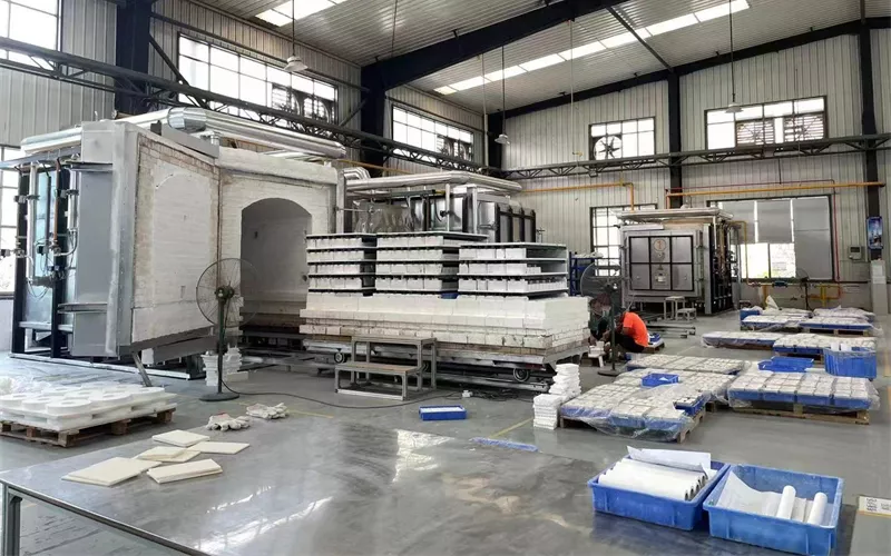
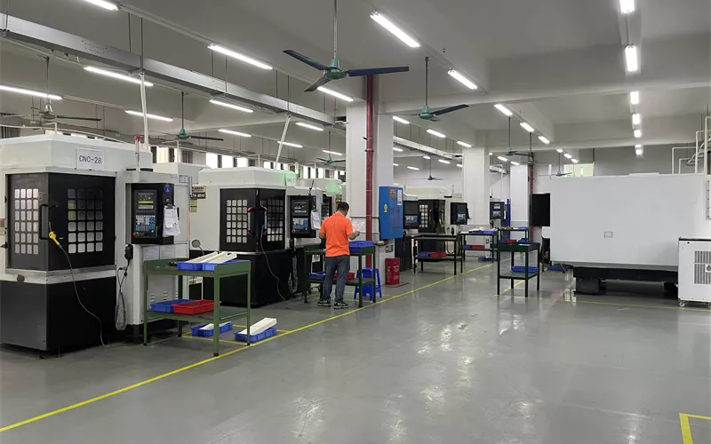
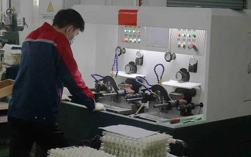
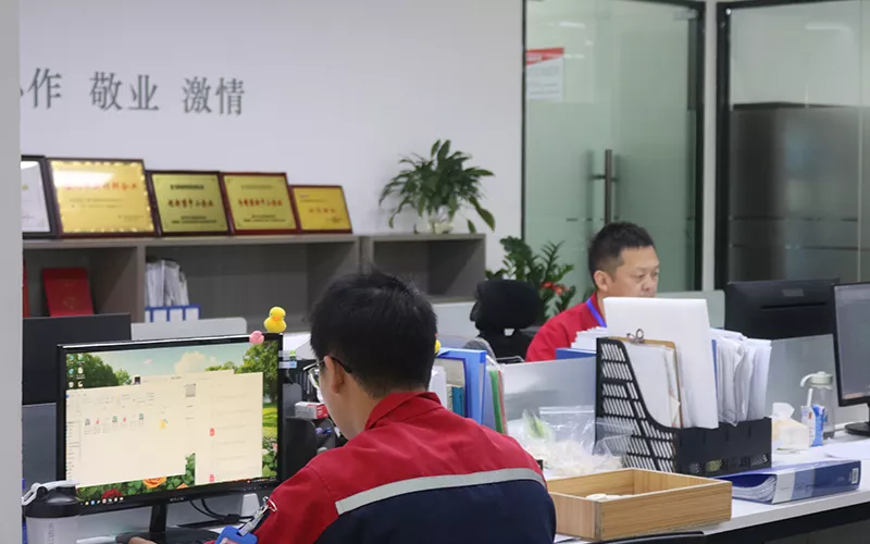
At GORGEOUS, quality control is our top priority. Every SiC substrate is manufactured to our customers’ exacting specifications and undergoes multiple inspections and tests, from raw materials to finished product, to ensure consistent performance and reliable quality.
당사의 생산 공장은 자동차 산업 품질경영시스템인 IATF 16949:2016 및 국제 표준 품질경영시스템인 ISO 9001:2015 인증을 획득하였습니다. 이는 품질에 대한 당사의 확고한 의지를 보여줄 뿐만 아니라, 고객에게 높은 수준의 맞춤형 솔루션을 제공할 수 있음을 보장합니다.
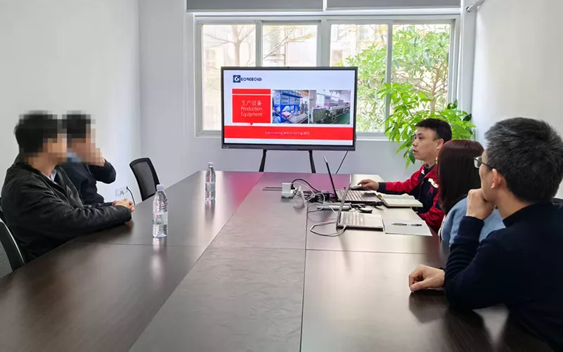
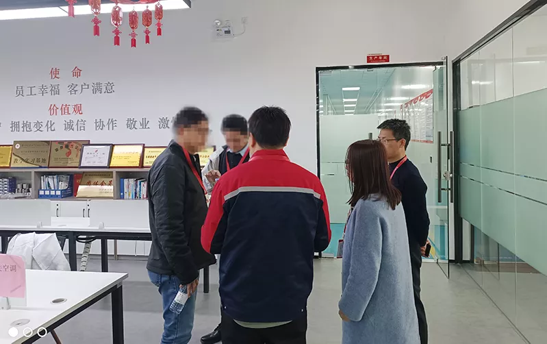
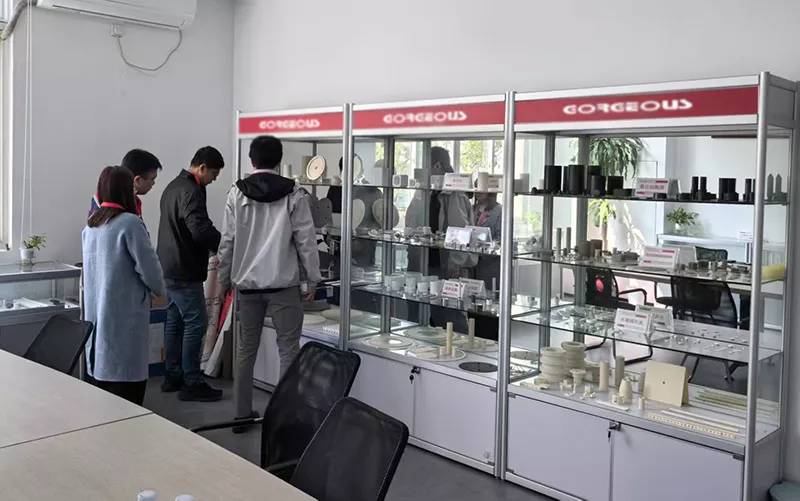
우리의 패스 성공 사례 추천사
The wafers provided by GORGEOUS are of stable quality, delivered on time and have excellent performance.

Christopher Johnson
We needed custom silicon nitride substrates for high-power electronic modules, and GORGEOUS fully met our technical requirements.

Richard Collins
The silicon nitride ceramic substrates provided by GORGEOUS have high surface finish, uniform microstructure and good performance consistency.

루카스 마이어
자주 묻는 질문
What is the heat dissipation performance of silicon carbide substrates?
SiC substrates typically have a thermal conductivity over three times that of silicon and can effectively reduce device operating temperatures. In high-power applications such as new energy vehicles and photovoltaic inverters, the use of SiC substrates enables long-term stable operation at high temperatures and high currents, effectively extending system life.
Is your delivery time stable?
Silicon carbide crystals are difficult to grow and process, which generally results in higher costs than silicon substrates. However, GORGEOUS’s production technology is highly mature, and we have a comprehensive production line and stable supply capabilities, supporting small-batch R&D to large-scale mass production, while ensuring stable delivery to customers.
Why is defect density in SiC substrates important?
Defect density (such as micropipes and dislocations) directly impacts chip yield and performance. Low-defect-density SiC wafers significantly improve device consistency and reliability, making them a key concern for customers during procurement.