SiC Wafers / SiC Substrates
GORGEOUS is a leading international ceramic supplier, specializing in providing customers with SIC substrates/wafer products used in new energy electric vehicles and semiconductor manufacturing. We can customize exclusive solutions based on the application!
Silicon Carbide Substrate Solutions
- Multi-Specification Wafer Supply: We offer standard wafer sizes, including 2-inch, 4-inch, and 6-inch, and can customize wafers based on customer needs.
- High-Purity Crystal Growth: We utilize advanced PVT (Physical Vapor Transport) and high-temperature sintering processes to ensure low defect density and high uniformity.
- 精密機械加工: We offer wafer dicing, grinding, polishing, and epitaxial (Epi) growth processes to ensure surface quality and flatness.
- Metallization and Post-Processing: We offer coating, ion implantation, patterning, and etching services tailored to customer needs to enhance device integration.
- Strict Testing: We conduct defect inspection, thickness uniformity testing, and surface roughness testing on every wafer to ensure it meets the diverse needs of our customers’ high-end applications.
Leading International SiC Substrate Supplier
GORGEOUS has over 15 years of expertise in high-performance ceramic substrate manufacturing, dedicated to providing customers with high-quality SiC substrates and wafers.
We utilize advanced crystal growth technology, employing high-temperature PVT, to produce large-scale, low-defect SiC crystals to meet global market demands.
We offer a complete processing chain, from crystal growth → wafer slicing → polishing → epitaxy → metallization, providing customers with a one-stop solution and ensuring consistent quality.
Our products are marketed globally and have earned the trust of numerous international customers. Whether you’re in the new energy vehicle, renewable energy, communications, or high-end semiconductor industries, GORGEOUS can meet your needs!
When you choose GORGEOUS, you’re not just choosing a supplier; you’re choosing a trusted manufacturing partner capable of large-scale production and fast delivery.
Silicon Carbide Substrate/Silicon Carbide Wafer Product Gallery
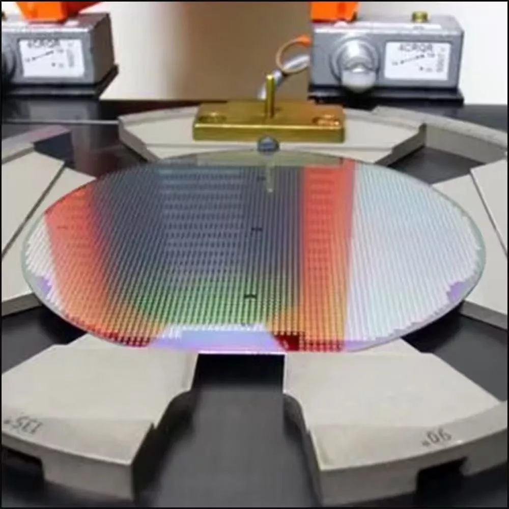
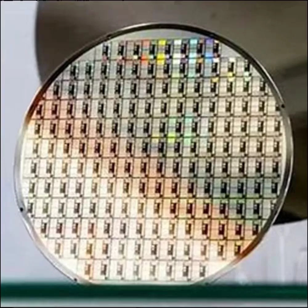
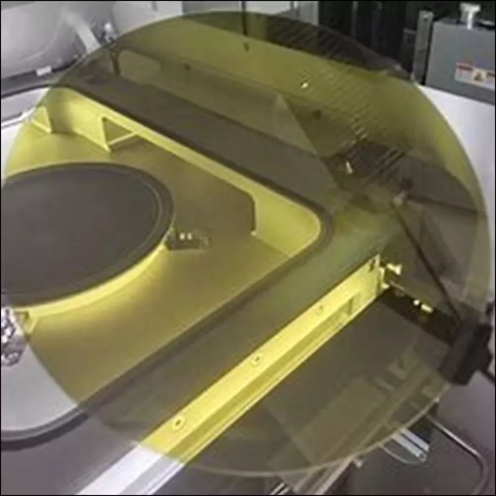
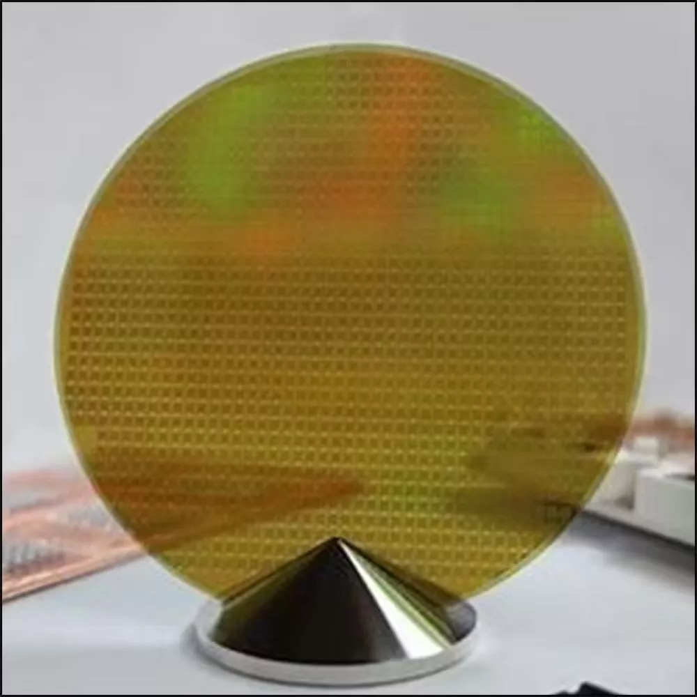
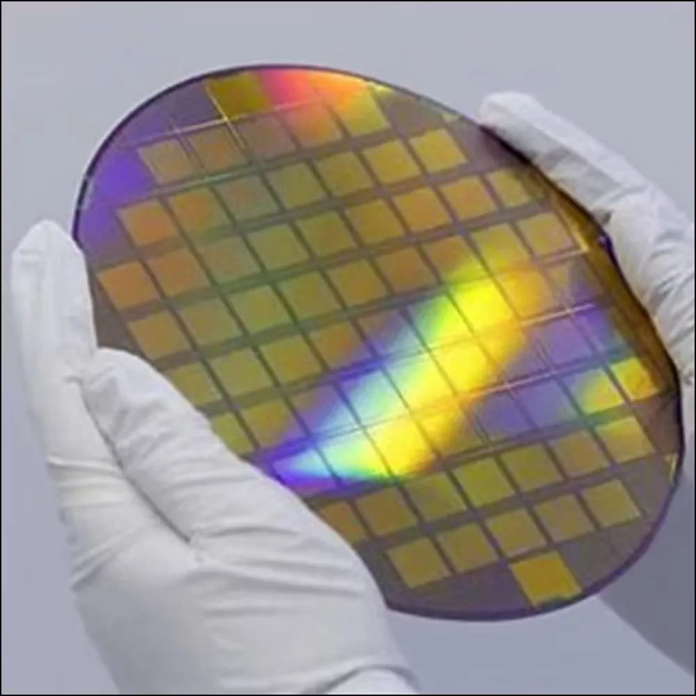
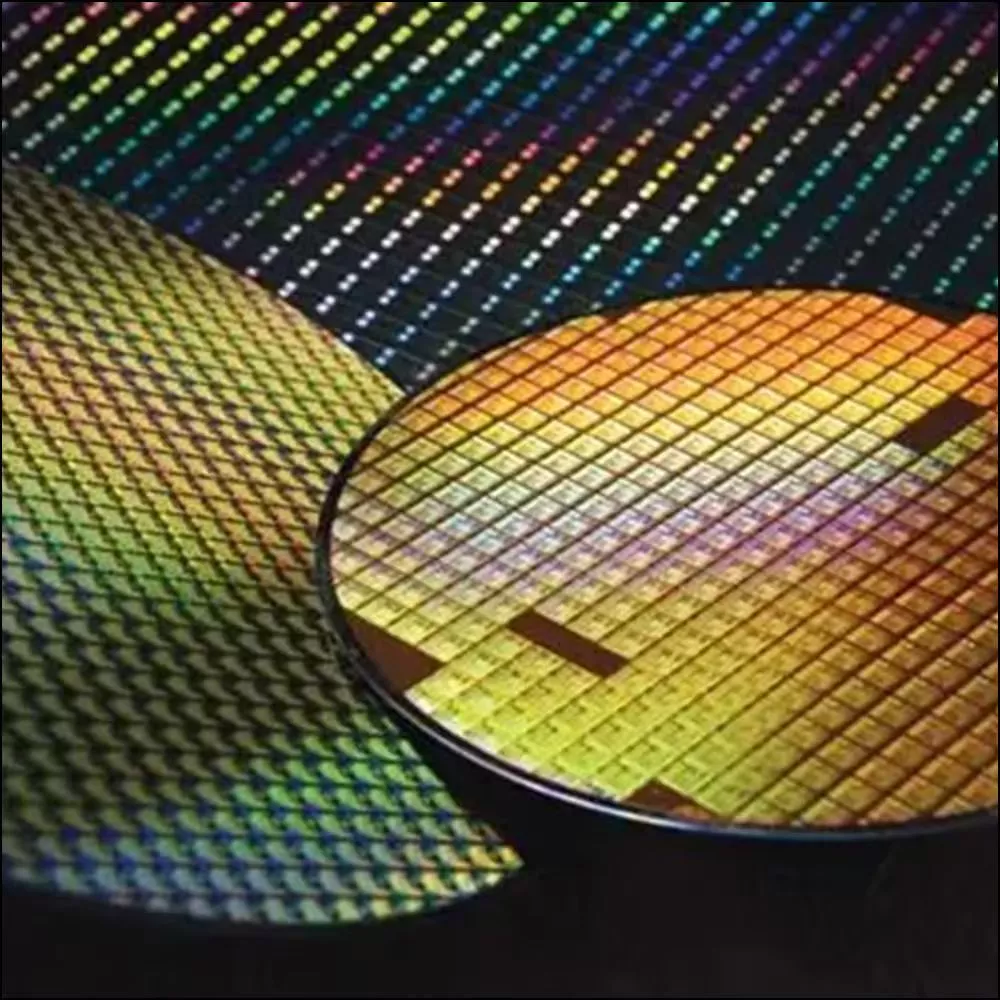
4H n-Type SiC Substrate
| Polytype | 4H |
| Diameter(mm) | 150/200 |
| Orientation(°) | 4 |
| Thickness(μm) | 350/500 |
| 表面仕上げ | Epi-ready |
4H Semi-Insulating
| Polytype | 4H |
| Diameter(mm) | 100 & 150 |
| Orientation(°) | 0 |
| Thickness(μm) | 500 |
| 表面仕上げ | Epi-ready |
Y
Silicon Carbide Substrate/Wafer Applications

Electronics and Semiconductor Fields
アルミナ基板は優れた電気絶縁性と放熱 properties(放熱 characteristic)を備えており、プリント基板(PCB)やハイブリッド集積回路(HIC)に使用できます。
エレクトロニクスおよび半導体分野におけるこれらの基板の主な用途には、半導体パッケージング用基板、厚膜/薄膜回路基板、センサーキャリアなどが含まれます。
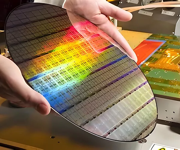
通信および高周波(RF)分野
アルミナ基板は、通信および高周波(RF)分野において、RF回路基板やマイクロ波デバイス基板として sensitive(最適)に使用できます。高周波通信(5G基地局やレーダーシステムなど)において、低い誘電損失と stable( stable/ stable/ stable)安定した信号特性を維持します。マイクロ波デバイス基板としては、 フィルター、パワーアンプ、カプラーなどの部品に多く採用され、優れた高周波 properties(高周波特性)を確保します。

自動車・新エネルギー分野
アルミナ基板は、自動車や新エネルギー車において、IGBTモジュールやモーター駆動モジュールなどのパワーモジュールの放熱用に使用され, システムの効率的かつ stable(安定)な動作を ensure(保証)します。また、車載用電子回路としても使用可能です。

照明およびディスプレイ分野
Alumina substrates can be used in high-power LED lamp beads to dissipate heat, helping to avoid light decay; while in laser diodes and displays, ceramic substrates can provide good electrical insulation and thermal management.

Aerospace and Military
Radar and satellite electronic devices require high-frequency, high-power, and highly reliable components, and alumina substrates can provide high insulation and thermal stability.
MOQ について心配ですか?
Our SiC substrates offer custom monolithic manufacturing to meet small order needs. Experience our services today.
GORGEOUSを選ぶ理由
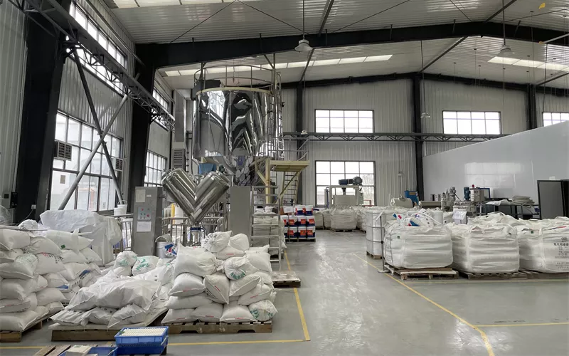
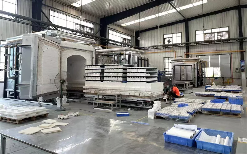
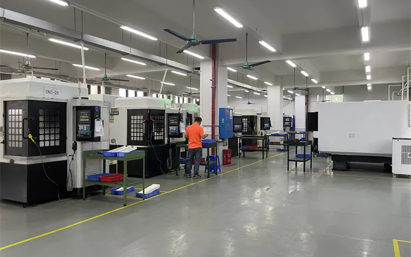
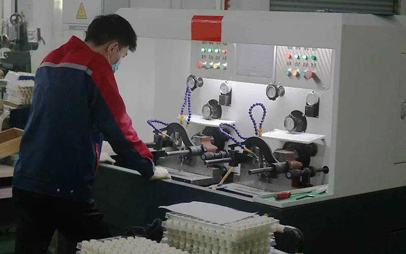
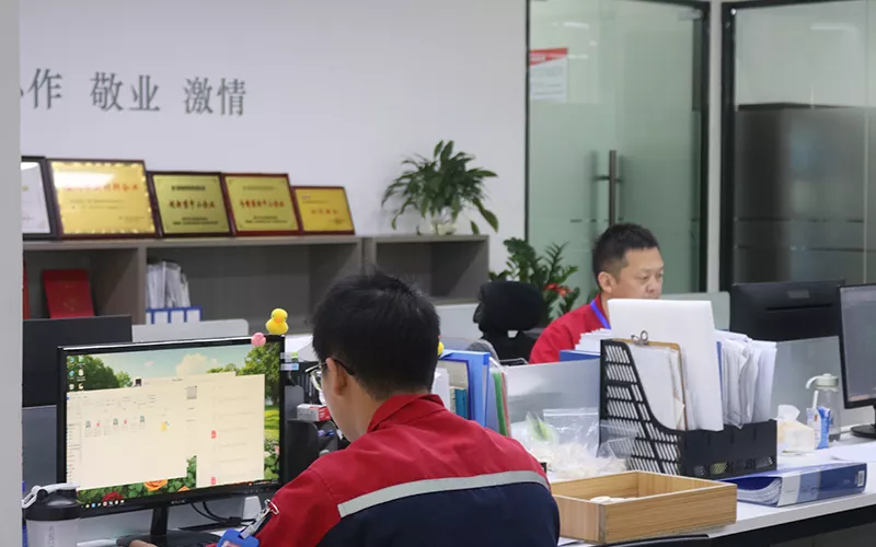
At GORGEOUS, quality control is our top priority. Every SiC substrate is manufactured to our customers’ exacting specifications and undergoes multiple inspections and tests, from raw materials to finished product, to ensure consistent performance and reliable quality.
当社の me (工場) は、自動車産業向けの IATF 16949:2016 および国際品質マネジメントシステムである ISO 9001:2015 の認証を取得しています。これは品質への取り組みを証明するだけでなく、お客様に高水準なカスタムソリューションを提供できることを保証するものです。
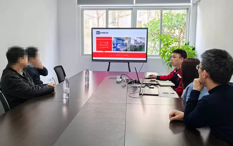
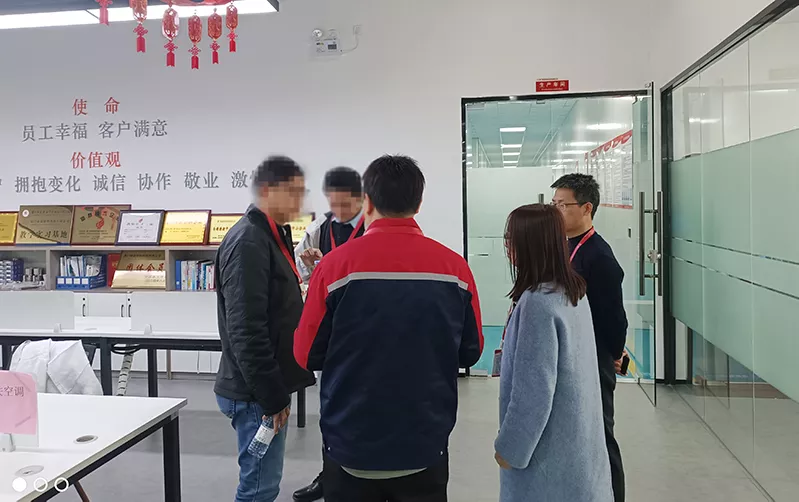
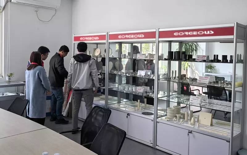
パス成功例 お客様の声
The wafers provided by GORGEOUS are of stable quality, delivered on time and have excellent performance.

Christopher Johnson
We needed custom silicon nitride substrates for high-power electronic modules, and GORGEOUS fully met our technical requirements.

Richard Collins
The silicon nitride ceramic substrates provided by GORGEOUS have high surface finish, uniform microstructure and good performance consistency.

ルーカス・マイヤー
よくある質問
What is the heat dissipation performance of silicon carbide substrates?
SiC substrates typically have a thermal conductivity over three times that of silicon and can effectively reduce device operating temperatures. In high-power applications such as new energy vehicles and photovoltaic inverters, the use of SiC substrates enables long-term stable operation at high temperatures and high currents, effectively extending system life.
Is your delivery time stable?
Silicon carbide crystals are difficult to grow and process, which generally results in higher costs than silicon substrates. However, GORGEOUS’s production technology is highly mature, and we have a comprehensive production line and stable supply capabilities, supporting small-batch R&D to large-scale mass production, while ensuring stable delivery to customers.
Why is defect density in SiC substrates important?
Defect density (such as micropipes and dislocations) directly impacts chip yield and performance. Low-defect-density SiC wafers significantly improve device consistency and reliability, making them a key concern for customers during procurement.