アルミナ基板
GORGEOUSは、エレクトロニクスおよび半導体製造分野で使用されるアルミナ基板製品のお客様への提供を専門とする、世界をリードするセラミックサプライヤーです。多様な純度およびサイズでのカスタム対応が可能です。
高品質アルミナ基板の製造
GORGEOUSは、純度99.6%のアルミナ基板をお客様に供給することができます。
当社では、薄膜および厚膜メタライズセラミック基板も提供しております。
製品の特長:
- 高い平滑性と極めて低い気孔率(ポーラス性)
- 反り、曲がり、うねりの最小化
- 高温環境における優れた物理的・化学的安定性
- Excellent insulation, high dielectric breakdown voltage, and high surface and volume resistivity
- 優れた機械的強度
- 耐油性・耐薬品性
アルミナ基板のグローバルリーディングカンパニー
GORGEOUSは、高性能セラミック基板の製造において15年以上の専門知識を有しており、アルミナ基板、PCB、薄膜セラミック基板を専門としています。当社の製品は、エレクトロニクス、パワーモジュール、LEDパッケージング、および先端半導体用途で幅広く me使用されています。
当社の高度な生産ラインと検査設備により、製造されるすべての基板が精度、信頼性、熱性能の最高水準を満たすことを保証します。原材料の processing( processing )から最終検査に至るまで、すべての工程で 엄격な品質管理が徹底されています。
当社の熟練したエンジニアチームがカスタム設計サポートと技術指導を提供し、お客様がパフォーマンスの向上と cost-effectiveness( cost 効率)の最適化を実現できるよう支援いたします。
GORGEOUSを選択することで、単なるサプライヤーにとどまらず、大規模生産と迅速な納品が可能な信頼できる製造パートナーを獲得できます。
アルミナセラミック基板/アルミナ基板PCB製品
お客様の多様なニーズにお応えするため、フレキシブル・アルミナ基板およびカスタム対応のアルミナPCBサービスを提供しています。
当社は、以下を含む高度な加工ソリューションを提供しています:
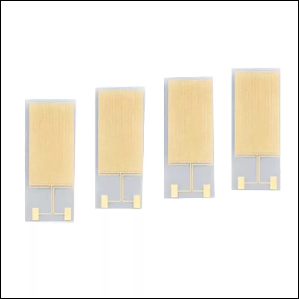
- 薄膜セラミック基板製造 – 精密表面処理と薄膜回路の集積
- メタライズ加工 – Mo/Mn+Niメッキ、タングステン系メタライズ、厚膜印刷など
- レーザー加工・スクライビング・穿孔 – 複雑な形状、スルーホール、高精度なマイクロ構造に対応
- 研磨および表面処理 – 優れた熱・電気的特性を実現する超平滑表面
- 基板実装・組立サポート – 電子部品の直接実装(ダイレクト・プレイスメント)を実現
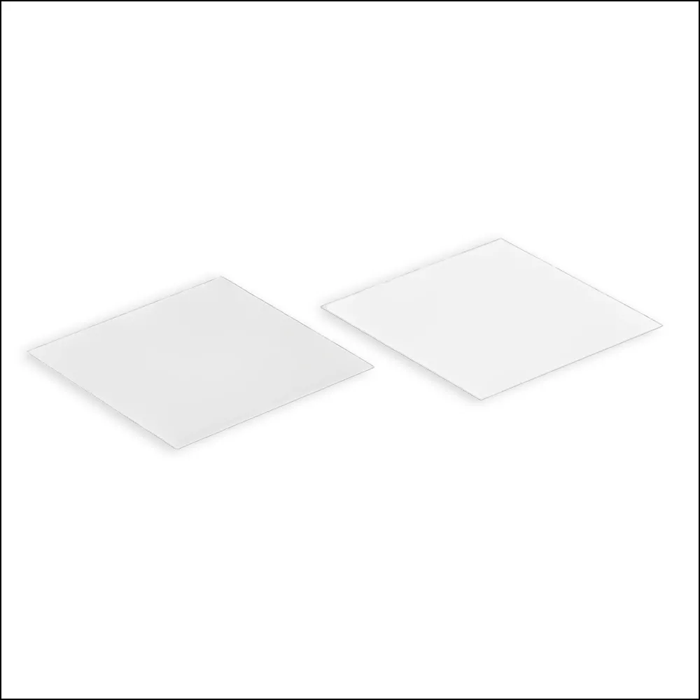
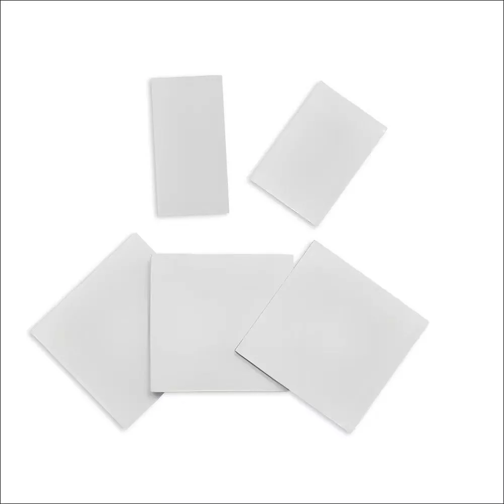
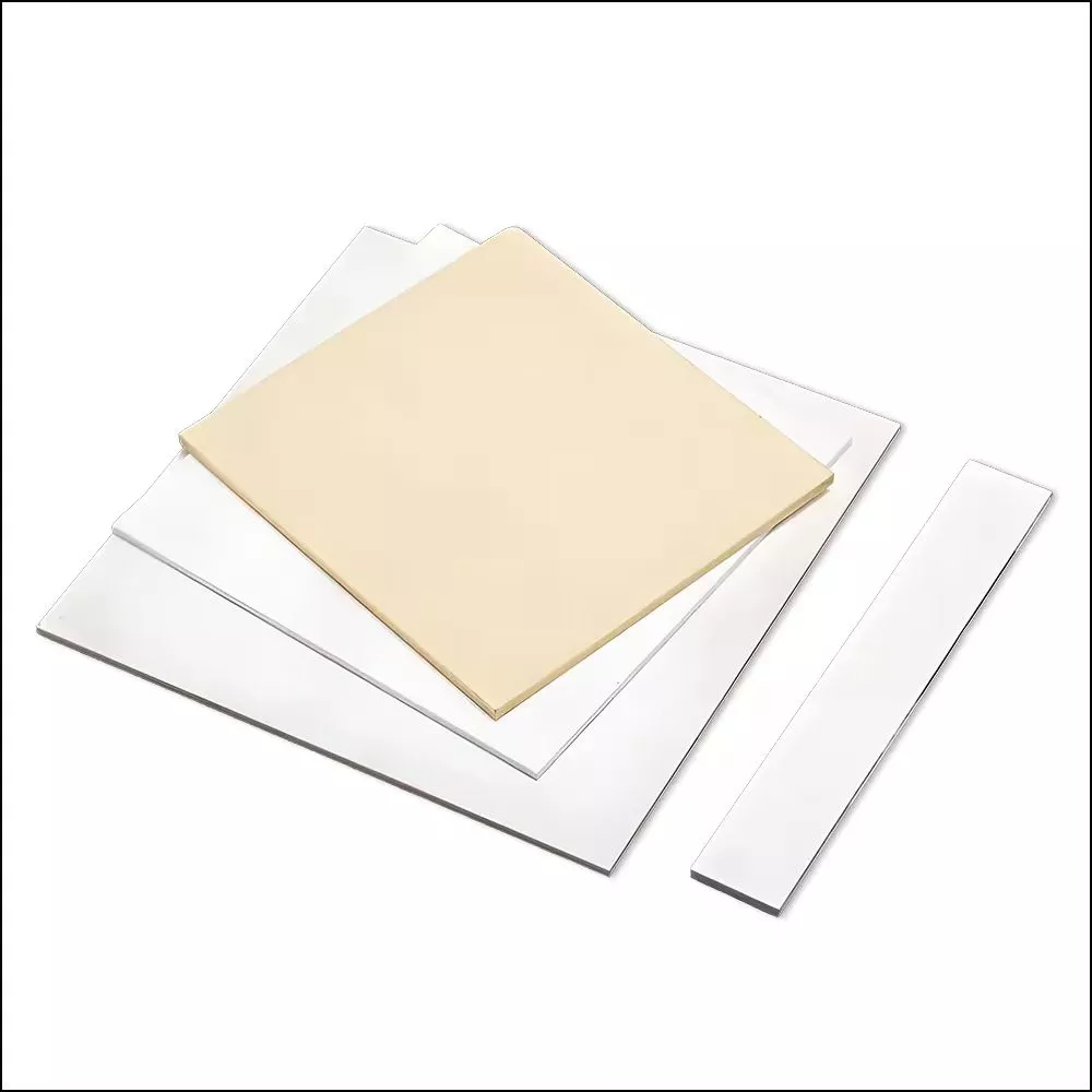
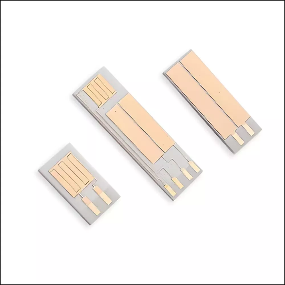
基板の標準サイズ
| 基板サイズ(mm) | 寸法誤差(mm) |
| 50.8*50.8 | ±0.2 |
| 76.2*76.2 | ±0.3 |
| 101.6*101.6 | ±0.4 |
基板の厚さ
基板の厚さは0.1~3mmで、標準厚さは0.254、0.381、0.508、0.635です。基板厚さの許容差は±10%です。
| 厚さ(mm) | 厚さ許容差(mm) | ||
| 焼成直後 | 地面 | 磨き上げられた | |
| 0.127 | ±0.012 | ±0.005 | ±0.005 |
| 0.254 | ±0.025 | ±0.005 | ±0.005 |
| 0.381 | ±0.038 | ±0.005 | ±0.005 |
| 0.508 | ±0.050 | ±0.01 | ±0.01 |
| 0.635 | ±0.063 | ±0.01 | ±0.01 |
| 0.762 | ±0.076 | ±0.01 | ±0.01 |
| 1.016 | ±0.10 | ±0.01 | ±0.01 |
技術的能力
| 基板タイプ | 表面粗さ | 反り |
| 焼成直後 |
前面: ≤100nm 背面: ≤200nm |
0.3% |
| 地面 | 顧客の要件に応じて | 0.1% |
| 磨き上げられた | ≤25nm | 0.1% |
アルミナ基板の用途
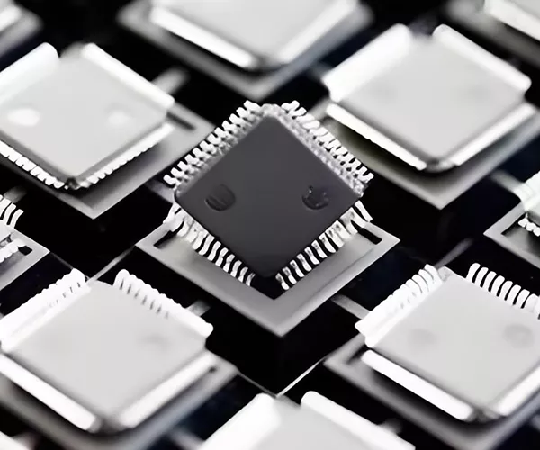
Electronics and Semiconductor Fields
アルミナ基板は優れた電気絶縁性と放熱 properties(放熱 characteristic)を備えており、プリント基板(PCB)やハイブリッド集積回路(HIC)に使用できます。
エレクトロニクスおよび半導体分野におけるこれらの基板の主な用途には、半導体パッケージング用基板、厚膜/薄膜回路基板、センサーキャリアなどが含まれます。

通信および高周波(RF)分野
アルミナ基板は、通信および高周波(RF)分野において、RF回路基板やマイクロ波デバイス基板として sensitive(最適)に使用できます。高周波通信(5G基地局やレーダーシステムなど)において、低い誘電損失と stable( stable/ stable/ stable)安定した信号特性を維持します。マイクロ波デバイス基板としては、 フィルター、パワーアンプ、カプラーなどの部品に多く採用され、優れた高周波 properties(高周波特性)を確保します。

自動車・新エネルギー分野
アルミナ基板は、自動車や新エネルギー車において、IGBTモジュールやモーター駆動モジュールなどのパワーモジュールの放熱用に使用され, システムの効率的かつ stable(安定)な動作を ensure(保証)します。また、車載用電子回路としても使用可能です。

照明およびディスプレイ分野
Alumina substrates can be used in high-power LED lamp beads to dissipate heat, helping to avoid light decay; while in laser diodes and displays, ceramic substrates can provide good electrical insulation and thermal management.

Aerospace and Military
Radar and satellite electronic devices require high-frequency, high-power, and highly reliable components, and alumina substrates can provide high insulation and thermal stability.
MOQ について心配ですか?
Our Al2O3 substrates offer a special minimum order quantity (MOQ) of one piece to meet small order needs. Experience our service now.
GORGEOUSを選ぶ理由
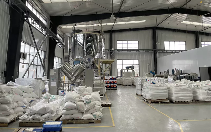
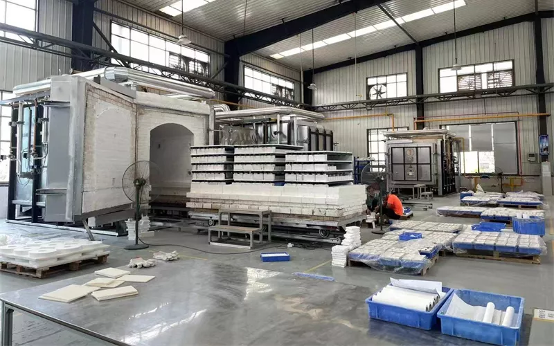
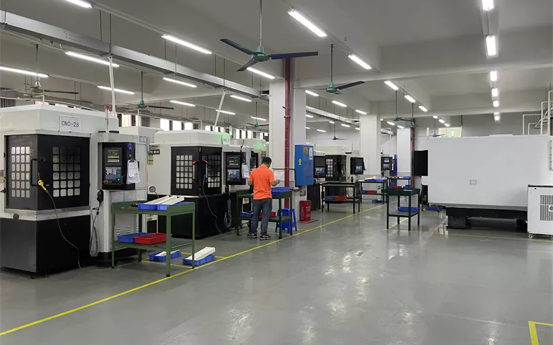
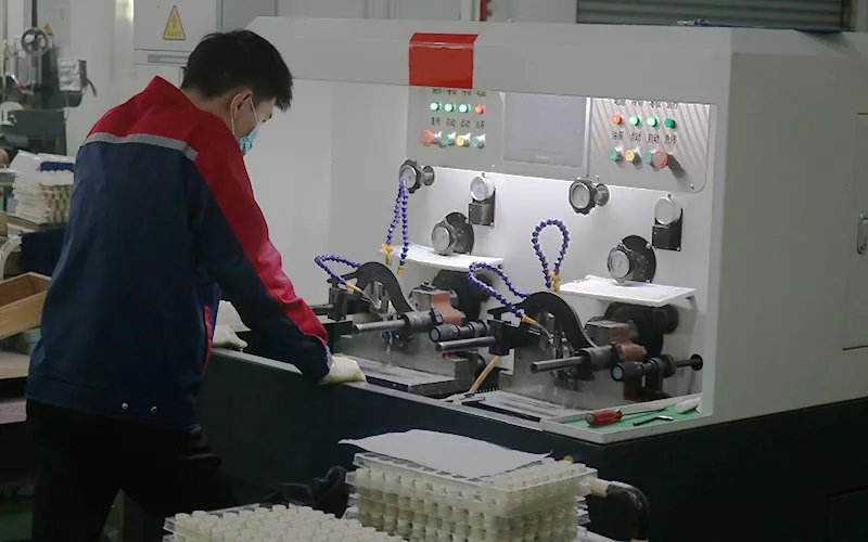
GORGEOUSでは、品質管理を最優先事項としています。すべてのアルミナ基板はお客様の厳密な仕様に基づいて製造され、原材料から最終製品に至るまで複数の検査と dedicated(専用)テストを実施し、一貫した性能と信頼性の高い品質を保証しています。
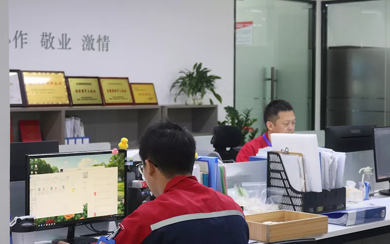
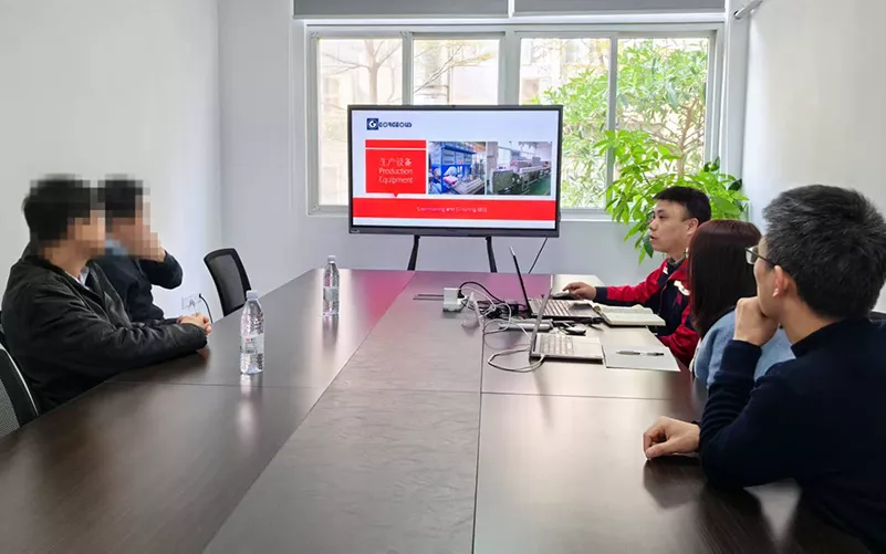
当社の me (工場) は、自動車産業向けの IATF 16949:2016 および国際品質マネジメントシステムである ISO 9001:2015 の認証を取得しています。これは品質への取り組みを証明するだけでなく、お客様に高水準なカスタムソリューションを提供できることを保証するものです。
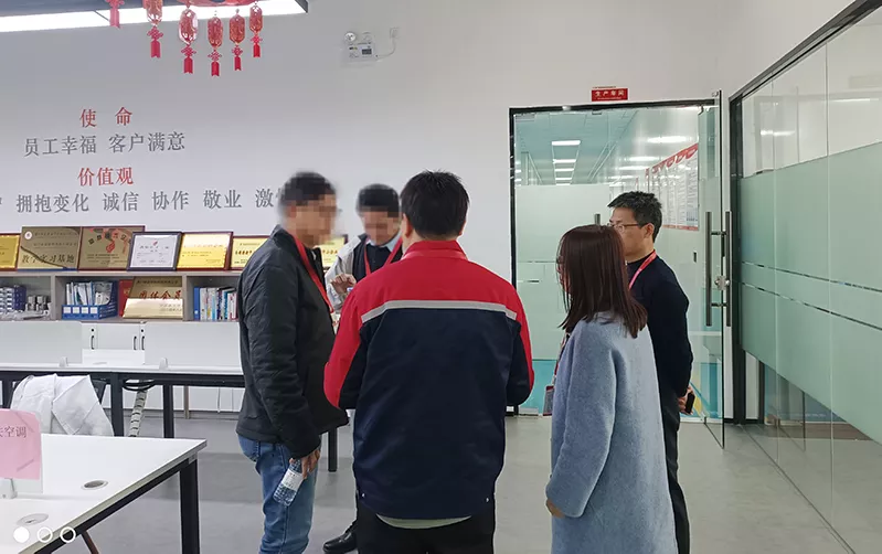
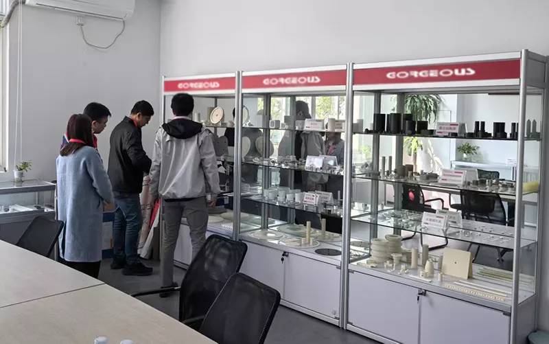
パス成功例 お客様の声
We are very satisfied with this batch of customized alumina ceramic substrates and the project is progressing very smoothly.

ジェームズ・ウォーカー
I believe we will continue to maintain this long-term cooperative relationship!

サラ・ウィルソン
The performance of GORGEOUS's alumina ceramic substrate exceeded our expectations and we were deeply impressed during the communication process.

Jonathan Miller
よくある質問
アルミナ基板とは何ですか?
Alumina substrate is a base material made primarily of aluminum oxide. It offers high insulation, high thermal conductivity, high-temperature resistance, corrosion resistance, and good mechanical strength. It is commonly used as a support material for circuits and as an insulating and heat-dissipating material.
What are the advantages of alumina substrates in electronic products?
They are relatively low-cost and cost-effective. They offer excellent electrical insulation, ensuring safe and stable circuits. Their high thermal conductivity facilitates heat dissipation and extends device life. They are also resistant to high temperatures and corrosion, making them adaptable to complex environments. Their exceptional mechanical strength allows them to support precision components.
Can GORGEOUS ceramic substrates be customized?
Yes, we offer custom ceramic substrates in various thicknesses, sizes, and surface finishes. We provide the best design and custom solutions based on our customers’ application needs.