알루미나 기판
GORGEOUS는 전자 및 반도체 제조 분야에 사용되는 알루미나 기판 제품을 고객에게 전문적으로 제공하는 세계적인 세라믹 공급업체입니다. 다양한 순도와 크기로 맞춤 제작이 가능합니다.
고품질 알루미나 기판 제조
GORGEOUS는 고객에게 99.6% 순도의 알루미나 기판을 공급할 수 있습니다.
당사는 박막 및 厚膜(후막) 메탈라이징 세라믹 기판도 함께 제공합니다.
제품 장점:
- 표면 평활도가 높고 포로시티(공기 구멍)가 매우 낮음
- 휨, 굽힘 및 물결 현상(ondulation)의 최소화
- 고온 환경에서의 우수한物理的·化學的 안정성
- Excellent insulation, high dielectric breakdown voltage, and high surface and volume resistivity
- 우수한 기계적 강도
- 내유성 및 내화학성
글로벌 선도 알루미나 기판 제조업체
GORGEOUS는 고성능 세라믹 기판 제조 분야에서 15년 이상의 전문성을 보유하고 있으며, 알루미나 기판, PCB 및 박막 세라믹 기판을 전문으로 합니다. 당사 제품은 전자, 파워 모듈, LED 패키징 및 첨단 반도체 응용 분야에 널리 사용되고 있습니다.
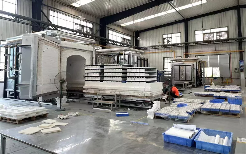
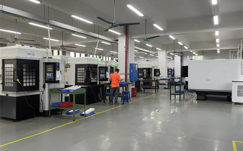
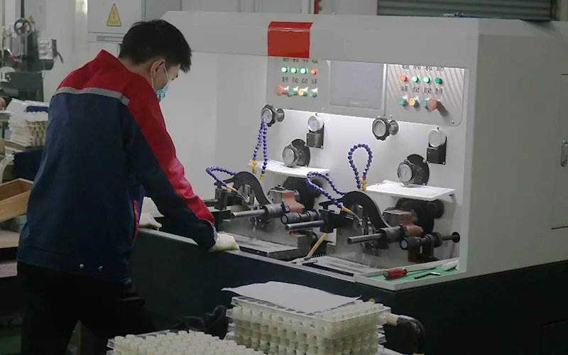
당사의 첨단 생산 라인과 시험 설비는 생산되는 모든 기판이 정밀도, 신뢰성 및 열적 성능에 있어 최고 수준의 표준을 충족하도록 보장합니다. 원자재 가공부터 최종 검사에 이르기까지 모든 공정이 엄격한 품질 관리를 거칩니다.
풍부한 경험을 갖춘 당사의 엔지니어 팀은 맞춤형 설계 지원과 기술 자문을 제공하여, 고객이 성능 향상과 비용 절감을 위해 솔루션을 최적화할 수 있도록 돕습니다.
GORGEOUS와 함께라면 단순한 공급업체를 넘어, 대규모 생산과 신속한 납품이 가능한 신뢰할 수 있는 제조 파트너를 얻게 됩니다.
알루미나 세라믹 기판 / 알루미나 기판 PCB 제품
당사는 다양한 고객 니즈를 충족하기 위해 유연한 플렉시블 알루미나 기판 및 맞춤형 알루미나 PCB 서비스를 제공합니다.
당사는 다음과 같은 첨단 가공 솔루션을 제공합니다:
- 박막 세라믹 기판 제조 – 초정밀 표면 처리 및 박막 회로 집적
- 메탈라이징(금속화) – Mo/Mn + 도금(Ni), 텅스텐 기반 메탈라이징 및 후막(thick film) 인쇄 등
- 레이저 가공 및 홀 뚫기(드릴링) – 복잡한 형상, 관통 홀 및 초정밀 미세 구조 구현에 적합
- 연마 및 표면 처리 – 우수한 열 및 전기적 성능을 위한 초평활 표면 구현
- 기판 조립 지원 – 전자 부품의 direct placement(직접 실장) 가능
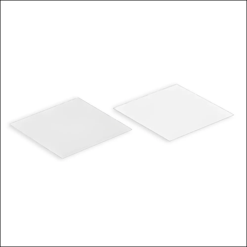
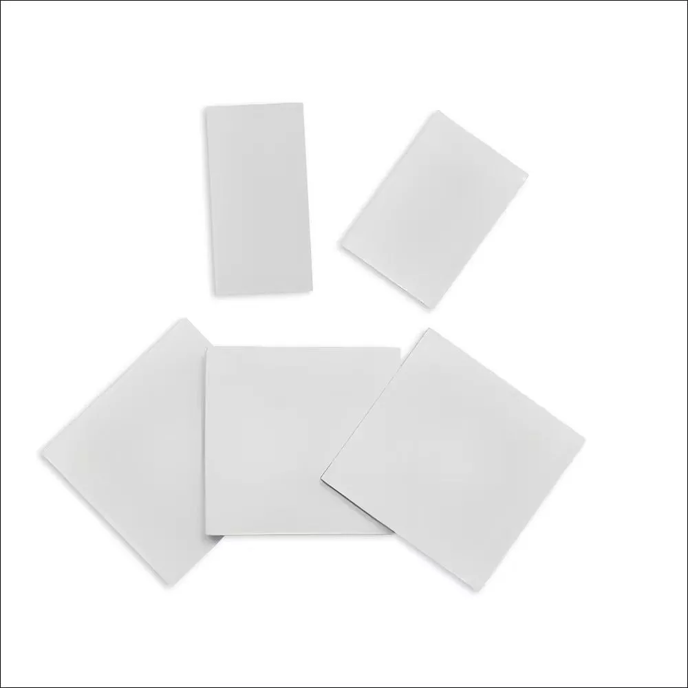
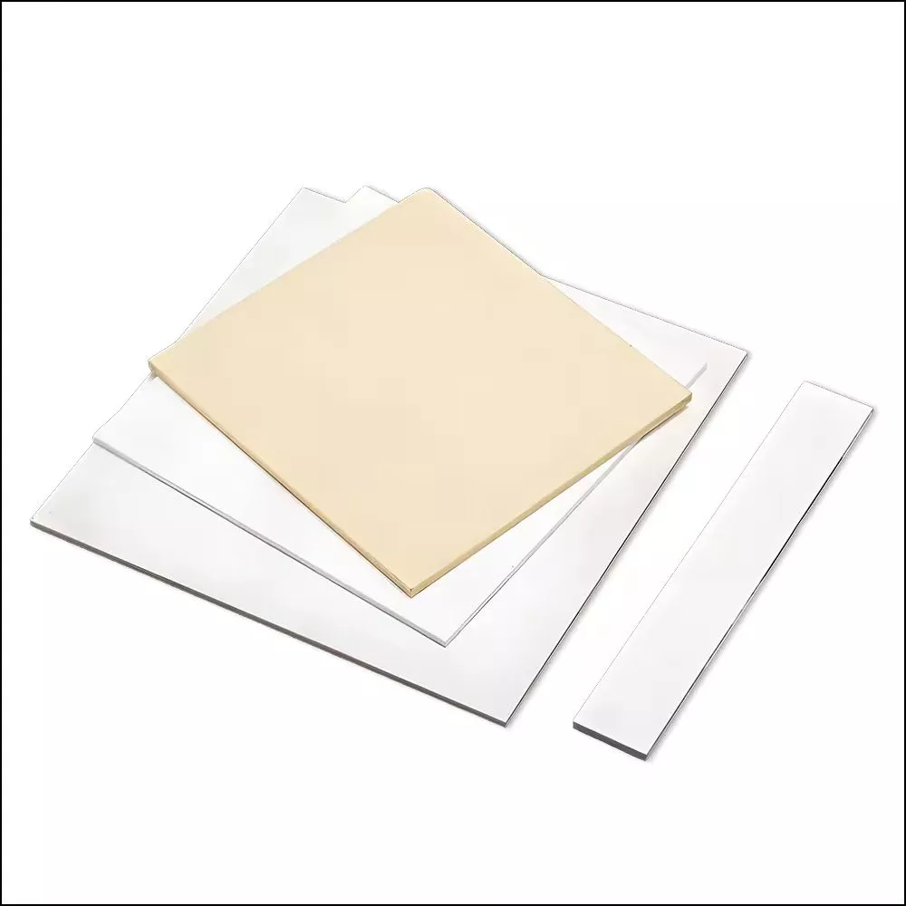
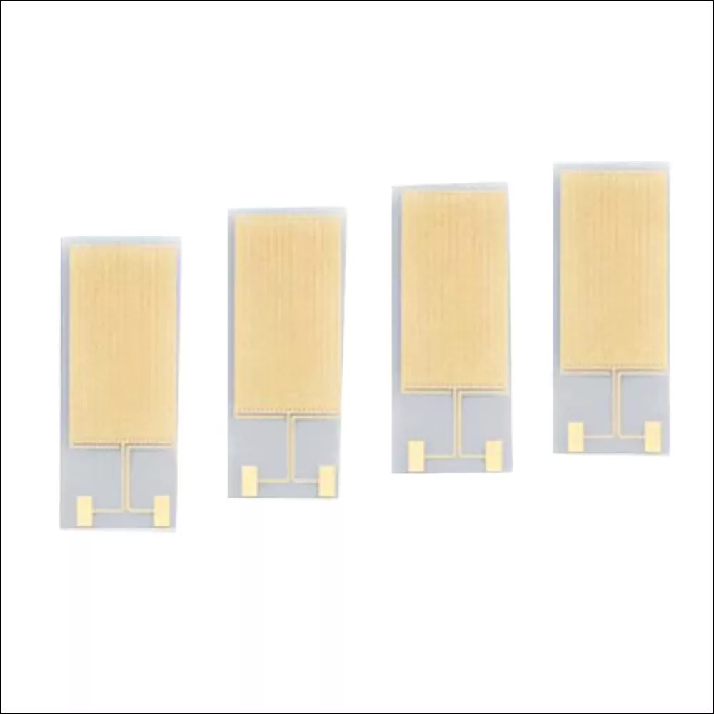
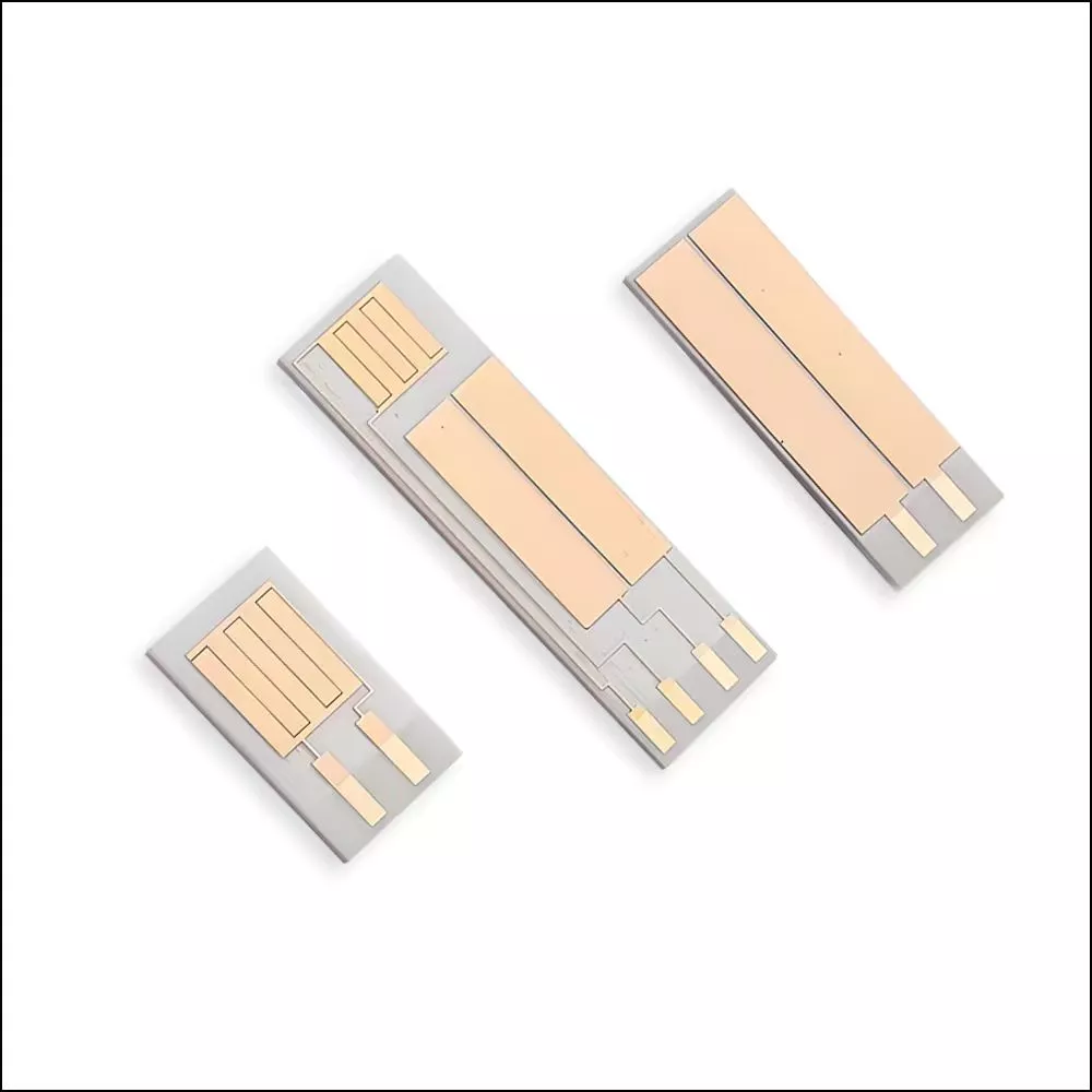
기판의 표준 크기
| 기판 크기(mm) | 치수 오차(mm) |
| 50.8*50.8 | ±0.2 |
| 76.2*76.2 | ±0.3 |
| 101.6*101.6 | ±0.4 |
기판 두께
기판 두께는 0.1~3mm이며, 일반적인 두께는 0.254, 0.381, 0.508, 0.635입니다. 기판 두께 허용 오차는 ±10%입니다.
| 두께(mm) | 두께 허용 오차(mm) | ||
| 발사된 상태 | 지면 | 우아한 | |
| 0.127 | ±0.012 | ±0.005 | ±0.005 |
| 0.254 | ±0.025 | ±0.005 | ±0.005 |
| 0.381 | ±0.038 | ±0.005 | ±0.005 |
| 0.508 | ±0.050 | ±0.01 | ±0.01 |
| 0.635 | ±0.063 | ±0.01 | ±0.01 |
| 0.762 | ±0.076 | ±0.01 | ±0.01 |
| 1.016 | ±0.10 | ±0.01 | ±0.01 |
기술적 역량
| 기판 유형 | 표면 거칠기 | 뒤틀림 |
| 발사된 상태 |
앞면: ≤100nm 뒷면: ≤200nm |
0.3% |
| 지면 | 고객 요구 사항에 따라 | 0.1% |
| 우아한 | ≤25nm | 0.1% |
알루미나 기판 응용 분야
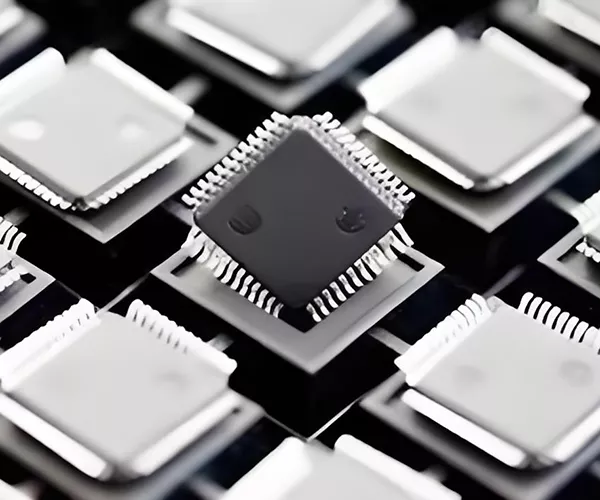
Electronics and Semiconductor Fields
알루미나 기판은 우수한 전기 절연성 및 방열 특성을 제공하며, 인쇄 회로 기판(PCB) 및 하이브리드 집적 회로(HIC)에 활용될 수 있습니다.
전자 및 반도체 분야에서 이러한 기판의 대표적인 응용 분야로는 반도체 패키징 기판, 두꺼운/얇은 박막 회로 기판, 센서 캐리어 등이 있습니다.
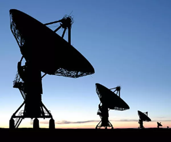
통신 및 무선 주파수(RF) 분야
알루미나 기판은 통신 및 무선 주파수(RF) 분야에서 RF 회로 기판 및 마이크로웨이브 소자 기판으로 활용될 수 있습니다. 고주파 통신(5G 기지국 및 레이더 시스템 등)에서 낮은 유전 손실과 안정적인 신호 품질을 유지합니다. 또한 마이크로웨이브 소자 기판으로서 필터, 전력 증폭기(PA), 커플러 등의 부품에 주로 사용되어 뛰어난 고주파 특성을 보장합니다.

자동차 및 신재생 에너지
알루미나 기판은 자동차 및 신에너지 차량에서 IGBT 모듈, 모터 드라이브 모듈과 같은 파워 모듈의 방열용으로 사용되어 시스템의 효율적이고 안정적인 작동을 보장합니다. 또한 차량용 전자 회로 기판으로도 활용될 수 있습니다.

조명 및 디스플레이
Alumina substrates can be used in high-power LED lamp beads to dissipate heat, helping to avoid light decay; while in laser diodes and displays, ceramic substrates can provide good electrical insulation and thermal management.

Aerospace and Military
Radar and satellite electronic devices require high-frequency, high-power, and highly reliable components, and alumina substrates can provide high insulation and thermal stability.
최소주문수량이 걱정되시나요?
Our Al2O3 substrates offer a special minimum order quantity (MOQ) of one piece to meet small order needs. Experience our service now.
왜 GORGEOUS를 선택해야 할까요?
GORGEOUS에서는 품질 관리를 최우선 과제로 삼고 있습니다. 모든 알루미나 기판은 고객의 정밀한 사양에 맞추어 제작되며, 원자재부터 최종 완제품에 이르기까지 다단계 검사와 테스트를 거쳐 일관된 성능과 신뢰할 수 있는 품질을 보장합니다.
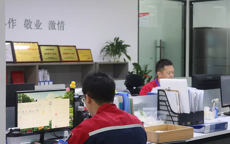
당사의 생산 공장은 자동차 산업 품질경영시스템인 IATF 16949:2016 및 국제 표준 품질경영시스템인 ISO 9001:2015 인증을 획득하였습니다. 이는 품질에 대한 당사의 확고한 의지를 보여줄 뿐만 아니라, 고객에게 높은 수준의 맞춤형 솔루션을 제공할 수 있음을 보장합니다.
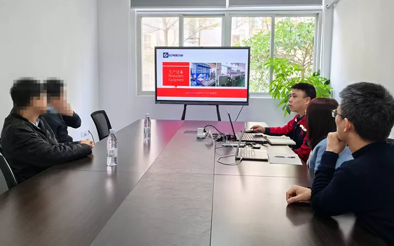
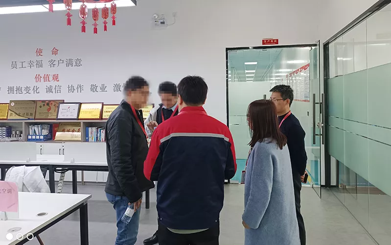
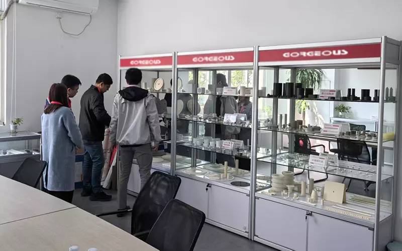
우리의 패스 성공 사례 추천사
We are very satisfied with this batch of customized alumina ceramic substrates and the project is progressing very smoothly.

제임스 워커
I believe we will continue to maintain this long-term cooperative relationship!

사라 윌슨
The performance of GORGEOUS's alumina ceramic substrate exceeded our expectations and we were deeply impressed during the communication process.

Jonathan Miller
자주 묻는 질문
알루미나 기판이란 무엇인가요?
Alumina substrate is a base material made primarily of aluminum oxide. It offers high insulation, high thermal conductivity, high-temperature resistance, corrosion resistance, and good mechanical strength. It is commonly used as a support material for circuits and as an insulating and heat-dissipating material.
What are the advantages of alumina substrates in electronic products?
They are relatively low-cost and cost-effective. They offer excellent electrical insulation, ensuring safe and stable circuits. Their high thermal conductivity facilitates heat dissipation and extends device life. They are also resistant to high temperatures and corrosion, making them adaptable to complex environments. Their exceptional mechanical strength allows them to support precision components.
Can GORGEOUS ceramic substrates be customized?
Yes, we offer custom ceramic substrates in various thicknesses, sizes, and surface finishes. We provide the best design and custom solutions based on our customers’ application needs.