半導体セラミックス
From wafer processing, vacuum adsorption, precision assembly to high temperature processes, GORGEOUS provides customers with one-stop customized semiconductor ceramic solutions.


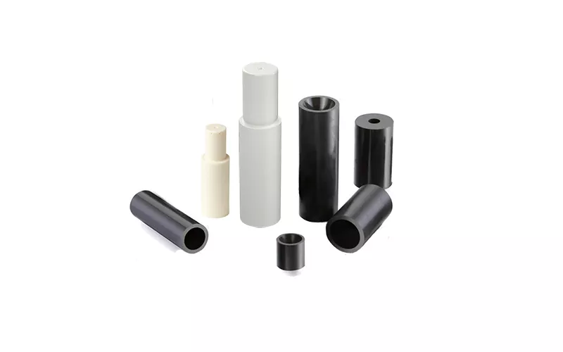


Precision Ceramic Structural Parts
Pan-Semiconductor Industry
Semiconductor Ceramics Description
Advanced ceramics are a critical part of semiconductor manufacturing equipment. A large amount of plasma is generated during the semiconductor manufacturing process, and it is crucial to use plasma-resistant materials as equipment components. Compared with metals, resins, and glass, advanced ceramics are more high-performance and reliable. Their resistivity is usually between conductors and insulators, and their electrical insulation is excellent, making them very suitable for semiconductor manufacturing processes.
We provide you with all the ceramic materials you need:
✅Alumina (Al2O3) — Ultra-high purity and rigidity;
✅Aluminum nitride (AlN) — Excellent thermal conductivity and insulation;
✅Silicon nitride (Si3N4) — Ultra-high fracture toughness and low thermal expansion coefficient;
✅Silicon Carbide (SiSiC)— Low density and coefficient of thermal expansion.
Based on your needs, we can recommend the best material for you to create ultra-high precision semiconductor ceramic components for you!
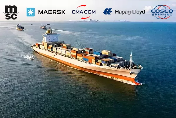
Guarantee Manufacturing & Shipping Time
GORGEOUS cooperates with several leading international logistics companies to produce for you quickly and deliver the products to you on time and intact!
The manufacturing and transportation of ceramics are affected by the process and your location. We will quickly manufacture them for you according to your plan and choose the best transportation method. Fastest air delivery in North America, arrives in 7 days.
The logistics companies we cooperate with include:
- MSC (Mediterranean Shipping Company)
- Maersk
- CMA CGM
- COSCO
- Hapag-Lloyd
- DHL
- UPS
- FedEx
- TNT
We work with multiple freight forwarders to guarantee you efficient shipping options at lower prices, on-time delivery, and no hidden fees!

Manufacturing

Packing

Loading
Transportation
Main Properties of Semiconductor Ceramics

高硬度

Wear-Resistant

Corrosion Resistant

耐高温性

Strong Insulation
GORGEOUS Customizable Product Accuracy Reference
| Processing Technology | parameter | Achievable accuracy |
| フライス加工 | Flatness, parallelism, Ra | Ra≥0,05 μm” Flatness<1μm |
| 研削 | Flatness | 5 μm < Ø 200 mm / 10 μm > Ø 200 mm |
| Roughness | Ra from 0,15 μm to 0,6 μm | |
| Parallelism | 5 μm < Ø 200 mm / 10 μm > Ø 200 mm | |
| Eroding | Symmetrical | Max. 0.05mm (hole/positioning slot) |
| 研磨 | Flatness, Parallelism, Roughness | Ra0.06μm-0.35μm Flatness<2μm Parallelism<2μm |
| Structuring | Roughness | Roughness < 3,2 μm Size < 150 μm |
*The specific accuracy needs to be determined according to the actual product material, shape and process requirements.

Semiconductor Ceramic Optional Process
| Product Type | Special Requests |
| セラミック基板 | Polishing, metallization coating, gold plating |
| セラミックアーム | Mirror polishing, ventilation slots, anti-static coating |
| Ceramic Rings/Gaskets | Sandblasting, Teflon coating, surface coating |
| セラミックチューブ | Inner wall polishing, hot isostatic pressing, surface coating |
| Ceramic Suction Cup | Micro hole processing, blind hole processing, adsorption vent design |
| Ceramic Heating Element | Metallized coating, surface glaze, antistatic coating |


Customized Semiconductor Ceramic Material Parameters and Selection

| Item | ユニット | 窒化シリコン |
| 密度 | g/cm3 | >3.2 |
| 硬度 | – | HRA90 |
| Vickers Hardness(Hv50) | HV0.5 | >1550 |
| Modulus of Elasticity | GPa | 290 |
| Flexural Strength | MPa | >600 |
| 圧縮強度 | MPa | 2500 |
| 破壊靭性 | MPam1/2 | >6.0 |
| Maximum Use Temperature | ℃ | 1200 |
| 熱伝導率 | W /(M·K) | 15-20 |
| 熱膨張係数 | 10-6 /℃ | >3.1 |
| Thermal Shock Resistance | △T℃ | 500 |
| Specific Heat Capacity | KJ/kg·K | 700 |
| 絶縁強度 | KV/mm | 1 |
| 誘電率 | εr | – |
| Volume Resistivity at 20℃ | Ω.cm | 1.0×10¹² |
| Item | ユニット | 加圧焼結炭化ケイ素 | Reaction Bonded Silicon Carbide | Recrystallized Sintered Silicon Carbide |
| 最大動作温度 | ℃ | 1600 | 1380 | 1650 |
| 密度 | g/cm3 | >3.1 | >3.02 | >2.6 |
| 気孔率 | % | <0.1 | <0.1 | 15% |
| 曲げ強度 | MPa | >400 | 250(20℃) | 90-100(20℃) |
| MPa | – | 280(1200℃) | 100-120(1100℃) | |
| 弾性係数 | GPa | 420 | 330(20℃) | 240 |
| GPa | – | 300(1200℃) | – | |
| 熱伝導率 | W/mk | 74 | 45(1200℃) | 24 |
| 熱膨張係数 | K-1×10⁻⁶ | 4.1 | 4.5 | 4.8 |
| ビッカース硬度 | GPa | 22 | 20 | – |
| Acid and Alkali Resistance | – | excellent | excellent | excellent |
| 財産 | ユニット | アル2お3 99.7 | アル2お3 99.5 | アル2お3 99 | アル2お3 95 |
| 純度 | — | 99.7% | 99.5% | 99% | 95% |
| 密度 | g/cm3 | 3.92 | 3.9 | 3.8 | 3.7 |
| 曲げ強度 | MPa | 375 | 370 | 340 | 304 |
| 圧縮強度 | MPa | 2450 | 2300 | 2250 | 1910 |
| 弾性係数 | GPa | 380 | 370 | 330 | 330 |
| 破壊靭性 | MPam1/2 | 4.5 | 4.3 | 4.2 | 3.8 |
| 硬度 | HRA | 91 | 91 | 90 | 89 |
| ビッカース硬度 | HV1 | 1600 | 1550 | 1450 | 1400 |
| 熱膨張係数 | 10- 6 K-1 | 7.8 | 7.8 | 7.7 | 7.5 |
| 熱伝導率 | W/mk | 32 | 32 | 25 | 25 |
| 熱衝撃安定性 | △T.℃ | 220 | 220 | 200 | 200 |
| 最大動作温度 | ℃ | 1750 | 1750 | 1700 | 1500 |
| 20℃における体積抵抗 | Ω·cm | 1015 | 1015 | 1014 | 1014 |
| 絶縁強度 | KV/mm | 22 | 20 | 16 | 15 |
| 誘電率(室温) | / | 10 | 11 | 11.5 | 11 |
| MHz誘電損失係数 | tan δ | 1×10⁻³ | 1×10⁻³ | 3×10⁻³ | 3×10⁻³ |
| Item | ユニット | 窒化アルミニウム |
| 密度 | g/cm3 | 3.31 |
| Modulus of Elasticity | GPa | 310 |
| 破壊靭性 | MPa × m1/2 | 3.5 |
| Poisson’s ratio | – | 0.25 |
| Compressive | MPa | 2100 |
| Flexural Strength | MPa | 335 |
| Hardness (Vickers) | GPa | 11 |
| Hardness (Knoop 100g) | Kg/mm2 | 1170 |
Customizable Ceramic Shaft end Type Reference

Alumina material products
❇️Wafer Polishing Plates:High hardness and wear resistance ensure high precision and long life of wafer polishing.
❇️End Effectors / Wafer-Handling:Excellent mechanical strength and chemical stability, suitable for wafer handling in high-cleanliness environments.
❇️Metalised Products:Good electrical conductivity and high temperature resistance, suitable for high power electronic devices.
❇️Chamber Rings / Sputtering Targets:High purity and corrosion resistance ensure the stability and consistency of the thin film deposition process.
Silicon Carbide Material Products
❇️Wafer Polishing Plates:Extremely high hardness and thermal conductivity, suitable for efficient and high-precision wafer polishing.
❇️Electrostatic Chucks:Excellent thermal conductivity and electrical insulation ensure stable adsorption of wafers at high temperatures.
❇️Vacuum Chucks:High strength and heat resistance, suitable for wafer fixing in high vacuum environment.
❇️End Effectors / Wafer-Handling:Lightweight and highly rigid, suitable for high-speed, high-precision wafer handling.
❇️Chamber Rings:Excellent high temperature and corrosion resistance, suitable for harsh semiconductor process environments.
What are The Uses of Semiconductor Ceramics?
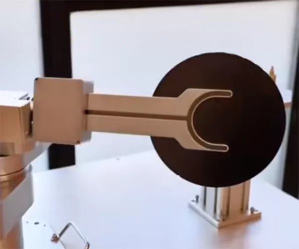
Ceramic Robot Arm/Ceramic End Processor
The ceramic arm plays the role of conveying and carrying in semiconductor equipment, which is equivalent to the arm of the robot of semiconductor equipment. It is mainly responsible for transporting wafers and silicon chips to designated locations.

Semiconductor Ceramic Heater
Semiconductor heaters have excellent thermal conductivity, high temperature resistance and electrical insulation. They can heat up quickly and evenly, and are widely used in semiconductor manufacturing, optoelectronic equipment and other scenarios.

Vacuum Wafer Ceramic Chuck
Vacuum wafer chuck is an important device for precision machining and semiconductor manufacturing, designed for fixing and handling silicon wafers or other thin materials. It can use the principle of vacuum adsorption to ensure that the wafer is stable and does not move during processing, testing or cleaning.

Semiconductor Equipment Parts
Many semiconductor devices use advanced ceramic products, such as ceramic insulating disks, ceramic insulating rings, thermistors, gas-sensitive ceramics, photosensitive ceramics, etc.
One-stop Semiconductor Ceramic Manufacturing Service
15+ 長年の経験。高精度とOEM設計。プロフェッショナルな研究開発チーム。競争力のある価格。
パス成功例 お客様の声

What is the service life of your products?
Our semiconductor ceramic products have excellent durability and can work stably for a long time in high temperature, high pressure and corrosive environments, reducing your replacement costs.
How to choose materials?
According to different application scenarios, we recommend you to choose the right material:
- Aluminum nitride (AlN): It has excellent thermal conductivity (>170 W/m·K) and electrical insulation, and is suitable for high-power semiconductor devices.
- Aluminum oxide (Al₂O₃): It has good mechanical strength and corrosion resistance and is widely used in conventional electronic components.
- Silicon nitride (Si₃N₄): It has both high temperature stability and impact resistance, and is particularly suitable for key components in harsh environments.
Your customization capabilities
We support customization of various specifications and complex structures. Whether it is micron-level precision processing or the manufacturing of special-shaped parts, we can meet your requirements.