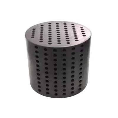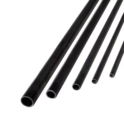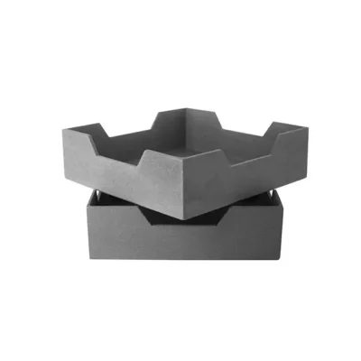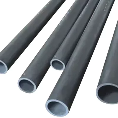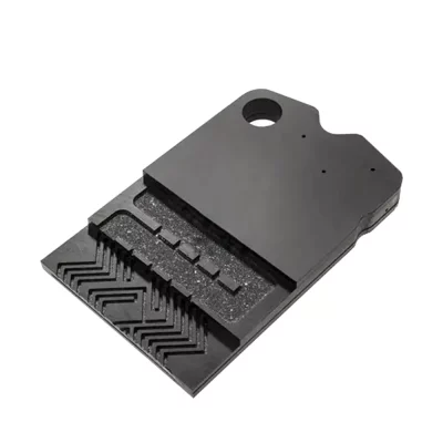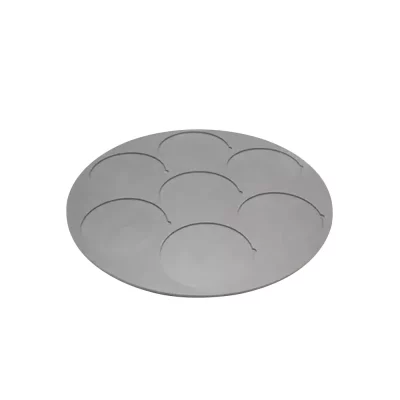
GORGEOUS CERAMICS (GGS) silicon carbide ICP carriers are made from spray-granulated silicon carbide powder, processed by isostatic pressing and high-temperature sintering.
We can precision machine the outer diameter, hole diameter, hole depth, and groove depth according to your drawings to meet your application requirements.
Quality Packaging and Cleanroom Protection Standards
Silicon carbide ICP carriers are highly precision components. They are extremely sensitive to microparticles and static electricity. Therefore, GORGEOUS CERAMICS (GGS Ceramic) uses Class 100 cleanroom packaging and multiple shockproof engineering seals. We guarantee that the product you receive will be free of contamination and damage throughout the entire process.
Ultra-clean Cleaning: Before leaving the factory, the silicon carbide ICP carriers undergo multiple ultrasonic pure water cleaning and hot air drying processes. We strictly control surface particle size and ion residue.
Double-layer vacuum antistatic packaging: All our packaging is completed in a Class 100 cleanroom and uses high-barrier double-layer vacuum antistatic PE bags to package the products.
Dedicated engraved card slots: We use high-density EPE foam or antistatic EVA to fully fit the contours of the carrier tray, preventing shaking and bumps during transportation.
Product Delivery Time
Upon receiving your drawings, we will complete an engineering assessment and quotation within 24 hours. Standard samples can be completed within 3-4 weeks, and complex custom-made parts can be delivered within 4-6 weeks. We also offer a green channel for your urgent orders, providing expedited production services.
Each batch of our carrier trays comes with a factory inspection report (CoC), including flatness, parallelism, coordinate measuring machine (CMM) dimensional measurement data, and material physical property test reports.
|
외경 |
용인 |
두께 |
용인 |
Chip size and number of chips |
|
380 |
±0.1 |
4.4 |
±0.05 |
4-inch (9 pieces), 6-inch (3 pieces) |
|
380 |
±0.1 |
3 |
±0.05 |
4-inch (9 pieces), 6-inch (3 pieces) |
|
330 |
±0.1 |
4.4 |
±0.05 |
4 inches (7 pieces), 6 inches (1 piece) |
|
330 |
±0.1 |
3 |
±0.05 |
4 inches (7 pieces), 6 inches (1 piece) |
Advantages of silicon carbide ICP carriers
Superior plasma resistance
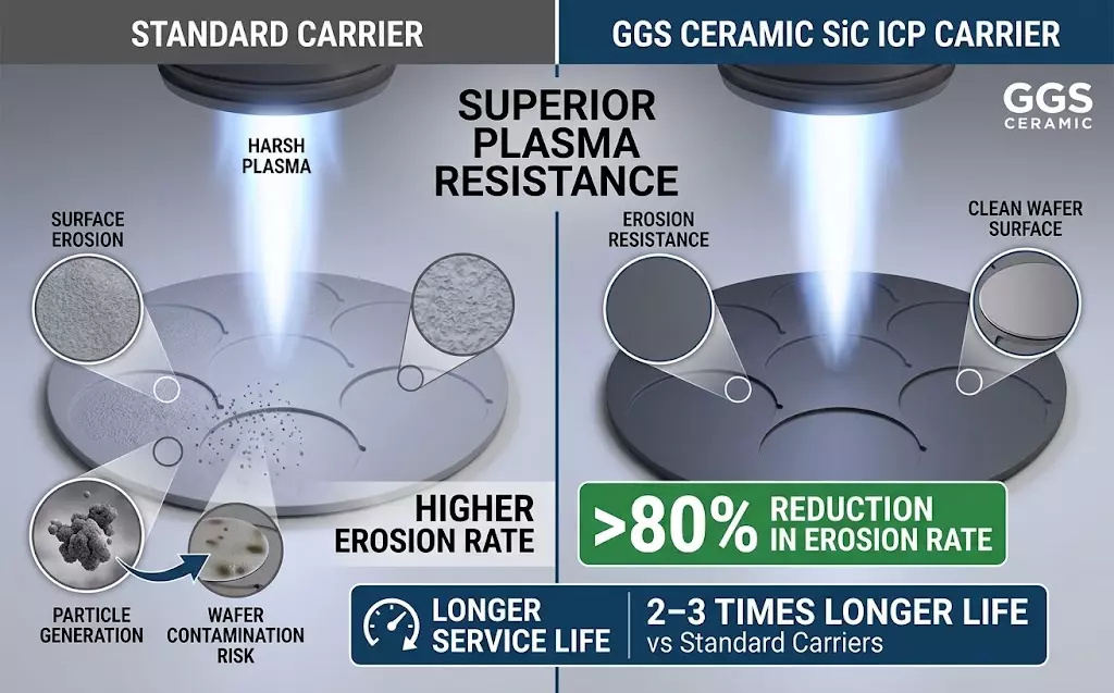
During ICP etching, plasma continuously bombards the surface of the carrier disk. Particles generated from the shedding of ordinary carrier disks can easily contaminate the wafer.
GORGEOUS CERAMICS (GGS Ceramic) silicon carbide ICP carrier disks, with their high purity, possess superior resistance to plasma bombardment.
- Etching rate reduced by >80%: Silicon carbide's extremely low material loss rate effectively resists continuous erosion by strong fluorine/chlorine-based plasmas.
- Lifespan extended by 2-3 times: Reduces the frequency of downtime for replacements.
우수한 열충격 저항성
In high-power ICP etching processes, the carrier pad faces significant thermal shock challenges. Insufficient thermal conductivity in the carrier pad manufacturing process can lead to localized heat accumulation and noticeable temperature differences. This temperature drift affects wafer yield.
GORGEOUS CERAMICS (GGS Ceramic) silicon carbide ICP carrier pads possess superior thermal conductivity comparable to metals.
- High thermal conductivity: Silicon carbide has a thermal conductivity ≥180, far exceeding that of ordinary ceramic materials, enabling instantaneous heat penetration and diffusion.
- Internal temperature difference control <1℃: Excellent thermal uniformity eliminates surface hot spots.
Excellent thermal shock resistance and thermal stability
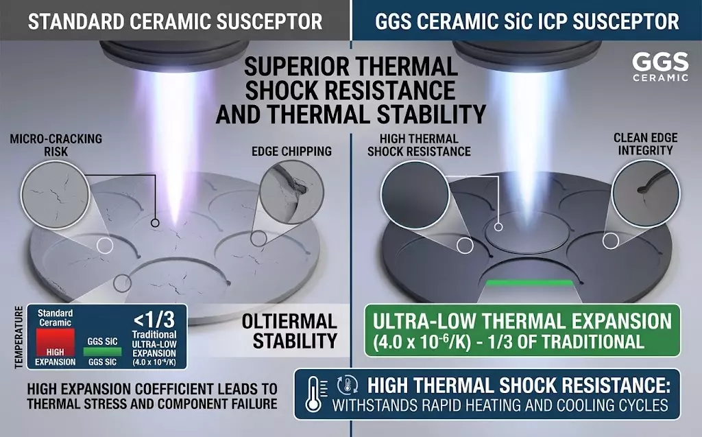
The frequent heating and cooling cycles of ICP equipment generate severe thermal stress. If the carrier pad has a high coefficient of thermal expansion or insufficient thermal shock resistance, microcracks can easily appear during wafer loading/unloading and power switching, leading to scrapping.
GORGEOUS CERAMICS (GGS Ceramic) silicon carbide ICP carrier pads possess extremely low coefficients of thermal expansion and high thermal conductivity.
- Ultra-low coefficient of thermal expansion: Silicon carbide has a coefficient of thermal expansion of 4.0 × 10⁻⁶ / K, only ⅓ of the traditional coefficient.
- High thermal shock resistance: The product can withstand extremely high heating and cooling rates, completely eliminating edge chipping and cracking caused by thermal stress.
Applications of silicon carbide ICP carrier disks
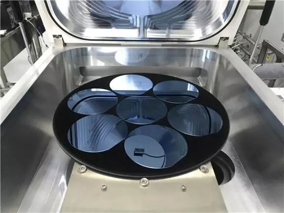
Silicon carbide (SiC) ICP carriers are core consumables in semiconductor inductively coupled plasma (ICP) etching, PSS etching, and epitaxial growth equipment.
GORGEOUS CERAMICS (GGS Ceramic) products can be customized to meet the needs of internationally renowned manufacturers.
- CoorsTek's PureSic® / CVD SiC Components series.
- SGL Carbon's SIGRACOAT® SiC-Coated Susceptors series.
- Ferrotec's Ferrotec CVD-SiC / Pure SiC Components series.
- Tokai Carbon's CVD SiC Coated Susceptor & Carrier series.
- Semicera Semiconductor's High Purity SiC Etching Carrier / Susceptor Series.
- VeTek Semiconductor's SiC Coating ICP/PSS Etching Carrier Series.
자주 묻는 질문
Will the micro-bump structure of the product crack or peel off due to thermal stress under thermal cycling?
No, our bump suction cup is manufactured through integrated sintering of a high-purity silicon carbide substrate, combined with a micron-level sandblasting process. The bumps and substrate are made of the same material, preventing thermal stress peeling or micro-cracks.
How resistant is the product to strong acids/alkalis and organic solvents?
Silicon carbide has excellent chemical inertness. When exposed to concentrated nitric acid, hydrofluoric acid mixtures, strong alkaline solutions, or various organic cleaning solvents, the surface will not experience chemical corrosion, fading, or micro-peeling.
Does GORGEOUS CERAMICS (GGS Ceramic) support 1:1 structural mapping and replacement?
Fully supported. We have extensive experience in secondary development and replacement verification. We can perform high-precision 3D mapping based on existing products or drawings, ensuring 100% compatibility of installation interfaces, gas path positions, and bump distribution with original equipment.
How to solve the problem of static electricity accumulation and wafer adhesion when using a chuck to pick up and unload wafers?
The problem of static electricity accumulation can be solved by controlling the bulk resistivity of the silicon carbide chuck within the specific range required by the customer through sintering processes and formula modulation.