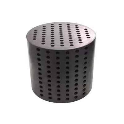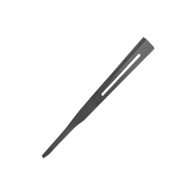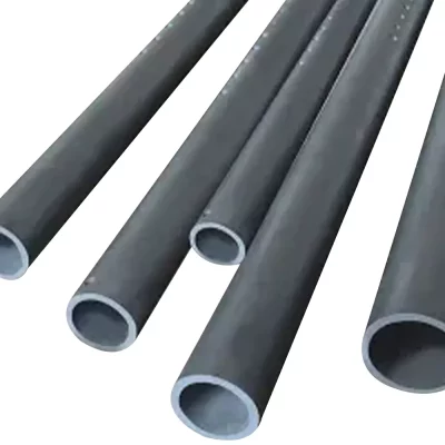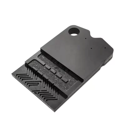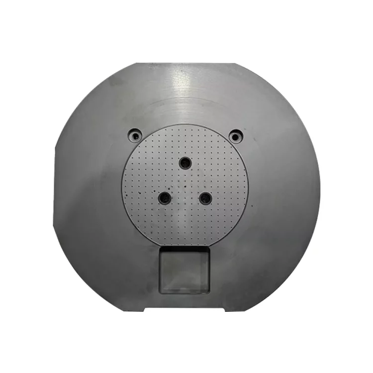
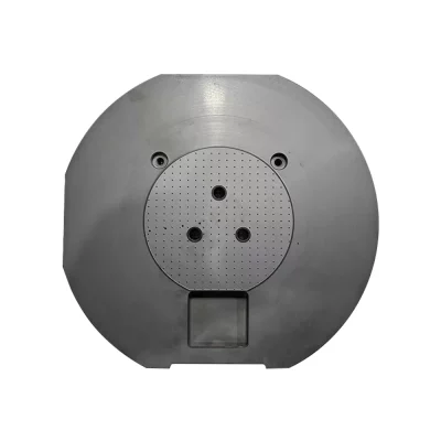
GORGEOUS CERAMICS (GGS Ceramic) manufactures silicon carbide bump vacuum chucks using spray-granulated silicon carbide powder, formed via isostatic pressing and high-temperature sintering. Precision machining is performed according to specifications, and a sandblasting process is used to create the bumps, ensuring the product meets operational requirements.
패키지
Semiconductor vacuum chucks demand near-stringent standards regarding surface particulate contamination; consequently, GORGEOUS CERAMICS (GGS Ceramic) enforces rigorous packaging requirements for its products.
Comprehensive Ultra-Clean Processing: Following micron-level precision machining and bump sandblasting, our vacuum chucks undergo multiple stages of deep ultrasonic cleaning and deionized water rinsing to thoroughly eliminate machining residues and micro-dust.
Double-Layer Vacuum Anti-Static Packaging: We package our products within a cleanroom environment using high-purity, double-layer vacuum anti-static bags, effectively blocking external air, moisture, and electrostatic interference.
Delivery date / Lead time
We offer highly competitive lead times, with delivery possible in as little as 2–3 weeks. For large-volume custom orders, we can complete full inspection and shipment within 4–6 weeks of drawing approval. We also provide a “green channel” for expedited production of urgent orders.
Advantages of Silicon Carbide Bumped Vacuum Cups
Ultra-high flatness of 0.3–0.5 μm
In nanoscale semiconductor manufacturing, even minute deviations on the surface of a vacuum chuck can cause localized wafer deformation, lithography defocus, and alignment errors.
Through ultra-precision polishing and micro-structuring processes, GORGEOUS CERAMICS (GGS Ceramic) achieves a flatness within the extreme range of 0.3–0.5 μm for its silicon carbide (SiC) bump chucks.
Effective reduction of wafer deformation: The combination of uniformly distributed micro-bumps and sub-micron flatness significantly minimizes stress concentration and localized indentation during wafer clamping.
Minimized particle contamination: By optimizing the contact area of the bump structure and leveraging the extremely low wear rate of silicon carbide, we reduce the retention and entrapment of particles.
Maintains accuracy despite temperature fluctuations; minimizes the impact of thermal stress
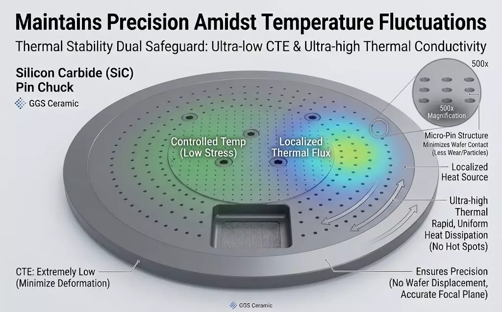
Some vacuum chucks are prone to minute deformation caused by thermal expansion and contraction, which can lead to wafer displacement or focal plane shifts. In contrast, silicon carbide—with its extremely low coefficient of thermal expansion and ultra-high thermal conductivity—provides a dual guarantee of thermal stability.
- Prevention of minute thermal deformation: When subjected to ambient temperature fluctuations and heat accumulation, our silicon carbide bump chucks exhibit minimal internal thermal stress, ensuring they do not undergo minute deformation due to thermal stress.
- High thermal conductivity for rapid heat dissipation: With a thermal conductivity of up to 160 W/(m·K), the silicon carbide bump chucks rapidly and uniformly disperse localized heat, preventing the formation of localized “hot spots” on the chuck surface.
Lightweight and highly rigid—designed specifically for high-speed motion and precision handling

As a moving component, the mass of the vacuum chuck determines the system’s inertia and load; however, prioritizing low mass alone can compromise structural rigidity.
Silicon carbide boasts exceptionally high specific stiffness. By employing lightweight structural design and integrated sintering technology, GORGEOUS CERAMICS (GGS Ceramic) reduces the mass of its silicon carbide bump chucks while delivering superior flexural rigidity and vibration resistance.
- Reduced equipment load: The lower mass of the chuck significantly alleviates the mechanical load on drive motors and guide rails, thereby reducing the risk of heat generation.
- Highly stable structure: Ensures the wafer remains secure and stable during high-frequency, high-acceleration handling and rotation.
자주 묻는 질문
How does the micro-bump design help reduce particle contamination on the wafer backside?
Particle entrapment on the wafer backside is a primary cause of defocusing and pattern distortion during lithography. GORGEOUS CERAMICS (GGS Ceramic) utilizes ultra-precision micro-machining to strictly control the contact area of the bump tops; this minimal contact area reduces the likelihood of particles being pressed onto the wafer backside.
Can you provide customized gas pathways and mounting structures for complex thermal environments?
Yes, GORGEOUS CERAMICS (GGS Ceramic) offers customization based on specific equipment requirements. This includes complex backside weight-reduction structures, internal micro-gas channels, multi-zone independent pressure-controlled suction holes, and various high-precision mechanical alignment holes meeting strict coaxiality and perpendicularity specifications.
Does the flatness of the chuck degrade after long-term use?
Silicon carbide possesses exceptional hardness and wear resistance. Combined with GGS Ceramic’s proprietary stress-resistant micro-bump structural design, the chuck resists surface wear and micro-indentations even after frequent wafer loading, unloading, and repeated vacuum clamping, ensuring long-term global flatness within the 0.3–0.5 μm range.