1.What to Expect From Silicon Carbide Wafers in 2026
Silicon carbide (SiC) wafers are soaring in demand in 2026 due to outstanding performance. They offer higher thermal management and efficiency in your high-temperature, high-voltage & frequency electronics than silicon wafers. Thus, your SiC wafers are now preferred in electric vehicles, 5G systems, and renewable energy systems.
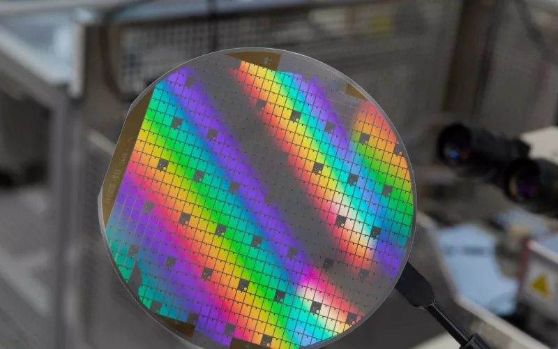
2. What Are Silicon Carbide (SiC) Wafers?
2.1 Definition of Silicon Carbide (SiC)
-
你的 碳化硅(SiC) is compound of carbon and silicon. Due to its exceptional hardness, wide bandgap, and resistance to high temperatures and voltages, SiC is preferred for robust electronics.
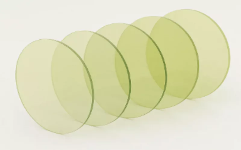
2.2 Definition of Silicon Carbide Wafers
-
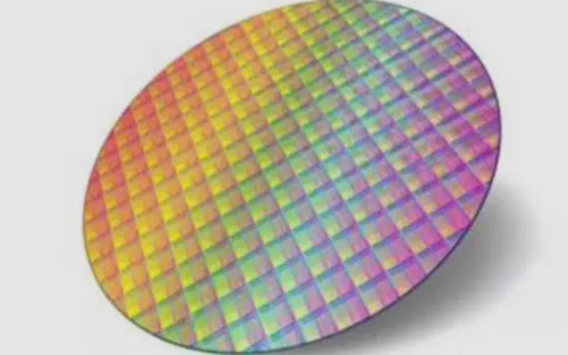
碳化硅 wafers are thin discs polished and cut from your SiC crystals. Your SiC wafers are the base substrate for fabricating high-performance semi conductors. For faster, highly efficient electronics in your industrial applications, choose silicon carbide wafers.
2.3 Silicon Carbide Vs Silicon Wafers
-
Silicon (Si) wafers have been the industry standard for general electronics. With a bandgap of 1.1 eV, they’re efficient for your conventional electronics, solar cells and low voltage applications.
-
Silicon carbide (SiC) wafers perform reliably in your high power electronics, electric vehicles (EVs), and RF devices. Your SiC offers a wide bandgap of 2.2-3.26 eV, 10x higher breakdown field, and 3x higher thermal conductivity.
3. Silicon Carbide Wafers Properties
3.1 What is the SiC Wafers Thermal Conductivity?
-
Your SiC (silicon carbide) wafers deliver exceptionally high 热导率 of 120 W/(m·K), and 3C-SiC reaching over 400 W/(m·K).
-
Due to the high thermal conductivity (ability to conduct heat), your power electronics dissipate heat excellently in small heat sinks.
3.2 How Wide is SiC’s Bandgap?
-
Your 4H-SiC offers a 3.26 eV bandgap, 6H-SiC delivers a 3.02 eV, and your 3C-SiC delivers 2.2-2.3 eV. This is wider than that of Si (1.1 eV).
-
The wider SiC bandgap allows your devices to operate at higher frequencies, voltages, and temperatures. Thus, SiC is ideal for your EVs and renewable energy systems.
3.3 Are Silicon Carbide Wafers Efficient?
-
Your silicon carbide wafers are highly efficient, offering 30%+ efficiency gains over conventional Si.
-
By managing heating better, handling more power, and offering faster switching, your SiC achieves smaller, lighter devices for your EVs.
3.4 Do SiC Wafers Withstand Extreme Heat?
-
Your SiC wafers withstand 1750°C+. While Si chips would quickly fail in your 5G communications and heaters, SiC wafers perform reliably in high temperatures.
-
The exceptional resilience makes SiC ideal for your high-heat applications.
3.5 How Hard and Strong are Your SiC Wafers?
-
Due to strong covalent bonding between silicon and carbon atoms, your SiC gets a 9-9.5 Mohs hardness.
-
Your silicon carbide offers a flexural strength of 450 ± 15 MPa and a fracture toughness of 4-6 MPa·m¹ᐟ².
3.6 To What Extent Are Silicon Carbide Wafers Chemically Inert?
-
Your silicon carbide (SiC) wafers are extremely chemically inert. They resist pH 1-6, pH 8-14, solvents, and oxidation at room temperature.
-
SiC’s excellent chemical stability makes it ideal for harsh environments in your aerospace and high-power applications.
Note: Silicon carbide can react with NaOH/KOH or chlorine at 900°C+.
3.7 What are the Benefits of SiC’s High Frequency Operation?
-
Your SiC wafers allow faster switching speeds, enabling operation at very high frequencies.
-
This reduces energy loss, minimizes the size of passive components, and improves system efficiency in your EVs, 5G, and solar.
3.8 Why Are SiC Wafers Ideal For High Voltage Applications?
-
Your SiC wafers offer a breakdown field of 2.8-3.5 MV/cm, 10 times higher than silicon’s 0.3 MV/cm.
-
With a high breakdown field, silicon carbide wafers withstand higher electrical fields in your high voltage applications.
Silicon Carbide Vs Silicon Wafers Key Technical Features Comparison
SiliconCarbideVsSiliconWafers_Table1.png
|
财产 |
Silicon Carbide (SiC) Wafers |
Silicon (Si) Wafers |
|
Thermal Conductivity (W/(m·K)) |
120 (with some prototypes reaching 400+) |
30 |
|
Bandgap (eV) |
2.2-3.26 |
1.1 |
|
Breakdown Field (kV/mm) |
3-3.5 |
0.3 |
|
Breakdown Voltage |
6kV+ (10x higher than Si) |
600V |
|
Operating temperature (°C) |
>1750 |
<600 |
|
效率 |
High (reduces energy loss by up to 30%) |
Good at lower power |
|
莫氏硬度 |
9-9.5 |
7 |
|
成本 |
Higher (100-200mm) |
Lower (300mm+) |
|
Switching Speed |
Faster (higher frequencies) |
慢点 |
Table: Comparison of the properties of silicon carbide wafers vs silicon wafers
Data source: Mater. Sci. Eng. 2025; 109(2): 021004; IEEE Trans. Compon. Packag. Manuf. Technol., vol. 12, no. 2, pp. 21004–21012, Feb. 2025
5. Silicon Carbide Wafer Manufacturing Process
5.1 Preparing Your Raw Materials
-
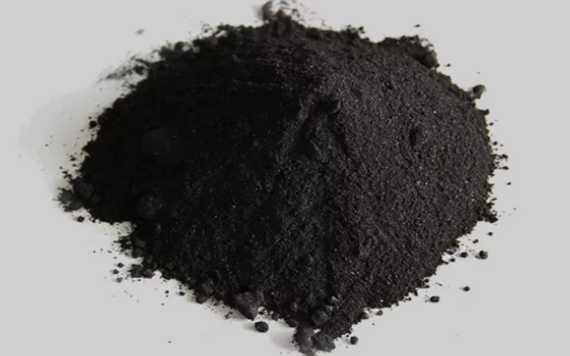
Your silicon carbide wafer production starts with mixing >99% purity silicon powder and carbon powder. Your SiC particles are then synthesized at 2000°C. After cleaning and crushing, your high purity SiC powder raw materials are prepared.
5.2 Crystal Growth
-
Using Physical Vapour Transport (PVT), your SiC powder is heated in a furnace. It’s vapourized and recrystallized onto a seed crystal. This forms your large SiC ingot.
5.3 Ingot Processing
-
Your obtained SiC ingot is cut into two wafers by diamond wire sawing. Your wafers are grounded and lapped to make them flat and remove damage caused during slicing.
5.4 Surface Finishing
-
Chemical Mechanical Polishing is used to get a smooth surface that helps improve your device quality. Etching is done to remove residual damage during mechanical processes.
5.5 Cleaning and Inspection
-
Your wafers are thoroughly cleaned with cleaning agent and pure water to remove surface dirt. Inspections for particles, flatness and defects ensure your silicon carbide wafers meet strict quality standards.
6. What Are Silicon Carbide Wafers Used For?
6.1 Automotive Applications
-
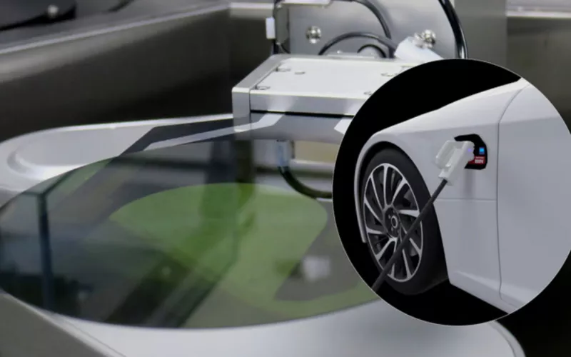
你的 electric vehicles (EVs) rely on silicon carbide wafers for high speed switching and low conduction losses.
-
Due to SiC’s efficiency, your EV’s battery stress is reduced and driving range is extended.
6.2 In Renewable Energy
-
你的 solar inverters and wind converters would experience 3x more thermal losses if Si wafers are used. SiC’s 6kV+ operating voltage supports larger power blocks with fewer parallel devices. Reliability and efficiency increase by up to 40%.
6.3 Power Electronics
-
In your 电力电子, conductive silicon carbide wafers offer fast switching and minimal leakage current. Due to higher breakdown voltage, your chargers and UPS systems benefit from compact designs.
6.4 In Telecommunications
-
Your 5G base stations would have slower speeds and interruption issues if Si wafers are used. Your high frequency silicon carbide wafers maintain signal integrity under continuous high-power RF transmission. With SiC, heat dissipation remains stable even at peak network times.
6.5 Aerospace Applications
-
Your conductive silicon carbide wafers tolerate radiation, extreme temperatures, and vibration in your aerospace systems. Your satellites and radar benefit from reduced failure rates.
6.6 High-Temperature Sensors and Abrasive Materials
-
Silicon would degrade if used in your industrial sensors. Because SiC supports gas sensing and pressure measurement your operation is reliable.
-
Your abrasive-grade SiC supports precision grinding and wear-resistant tooling.
“We’ve been using 4H-SiC wafers in our electric vehicle manufacture for the last 5 years now. Energy losses are always below 1%, and they effectively handle our 800V EV architecture.” — Xiyang Z., Power Electronics Engineer, Hyundai
7. Silicon Carbide Wafer Market Growth
7.1 Silicon Carbide Wafer Market Size in 2026
-
Your silicon carbide wafer market is expanding at double digits in 2026. The demand is driven by adoption of your EV models, fast-charging infrastructure, and renewable installations.
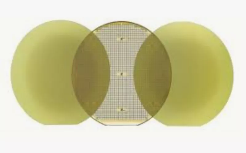
7.2 Transition to 200mm Silicon Carbide Wafers
-
By transitioning from 150 to 200mm silicon carbide wafers, your industry reduces cost per device. With larger wafer diameter, your manufacturing efficiency increases by 20-30%.
7.3 Future Trends in Your SiC Wafers
-
Future silicon carbide wafer production focuses on lower defect density and ensure improved uniformity.
-
Crystal growth and device fabrication vertical integration increases supply reliability. Wafer sizes are further transitioning from 200mm to 300mm.
8. Selecting Your Silicon Carbide (SiC) Wafers
8.1 Which Types of SiC Wafers Are Preferred?
-
4H-SiC offers superior electron mobility for your high-power devices.
-
6H-SiC is used in your high-brightness LEDs and RF microwave devices due to its good optical properties.
-
Your N-type SiC is doped with nitrogen, creating excess electrons. They’re used in your power switches and inverters.
SiliconCarbideWaferTypes_Table2.png
|
SiC Wafer Type |
Key Property |
应用 |
|
4H-SiC |
High electron mobility |
EV inverters |
|
6H-SiC |
Stable optical properties |
LEDs, RF microwave device |
|
N-type SiC |
Electron-rich conductivity |
Power switches |
|
P-type SiC |
Hole-based conduction |
Junction devices |
|
High Purity Semi-Insulating (HPSI) SiC |
High resistivity |
RF and microwave substrates |
|
3C-SiC |
Cubic structure |
Experimental electronics |
“After switching from silicon to 4H-SiC wafers in our charging modules, thermal margins improved by 40%.” — Chen R., Systems Integration Lead, Infypower
8.2 What Certifications to Check for Quality?
-
Your silicon carbide (SiC) wafers should meet SEMI (Semiconductor Equipment and Materials International) material standards. Also verify ASTM F1241 & C1835 and ISO 9001 & 14001 product standards for quality.
8.3 Where to Buy Silicon Carbide Wafers
-
Buy silicon carbide wafers from manufacturers or suppliers who guarantee vertically controlled crystal growth. China silicon carbide wafers wholesale suppliers offer competitive pricing at scale.
在 GGSCERAMIC®, we offer ISO-certified 碳化硅陶瓷 with documented wafer traceability and technical assistance.
9. FAQs About Silicon Carbide Wafers
Q1: What are silicon carbide wafers used for?
A: Your silicon carbide (SiC) wafers are used in high-power electronics, EV systems, RF devices, and renewable energy converters.
Q2: What’s driving the growth in the silicon carbide wafer market in 2026?
A: The sustained demand growth is as a result of EV electrification, renewable expansion, and high-efficiency power conversion.
Q3: What are the advantages of the 200mm silicon carbide wafers?
A: Your larger wafers reduce cost per die and align with mature semiconductor manufacturing tools.
Q4: How are silicon carbide wafers made?
A: The silicon carbide wafer manufacturing process uses PVT crystal growth, slicing, polishing, and precision inspection.
Q5: What are the challenges in the manufacture of conductive silicon carbide wafers?
A: Technical challenges in your SiC wafer production include doping uniformity and defect control.
Q6: Which is more expensive between silicon carbide vs silicon wafers?
A: Your silicon carbide wafers cost more than Si due to crystal growth complexity and lower yield at large diameters.
结论
Your silicon carbide wafers’ performance under heat, voltage, and frequency define the 2026 material demand requirements. Market growth follows technical necessity, and SiC is still preferred over Si for efficient, durable electronics.