Ceramics are an invaluable raw material for many industries today. For entities specializing in flexible electronics, керамические материалы provide a robust foundation for attaching electronic components.
Ceramic materials substrates demonstrate unique mechanical strength, outstanding thermal conductivity, high electrical insulation and stress endurance, and superior fracture toughness.
In this article, we explore the science behind ceramic substrates, their applications, and their significance in modern technology.
Что такое керамические подложки?
А керамическая подложка is a material used as a base or support material to which other components are attached.
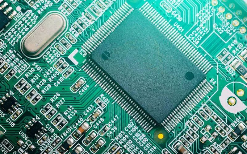
In electronic packaging, a ceramic substrate is used as an insulating layer between a printed circuit board (PCB) or lead frame and a semiconductor die.
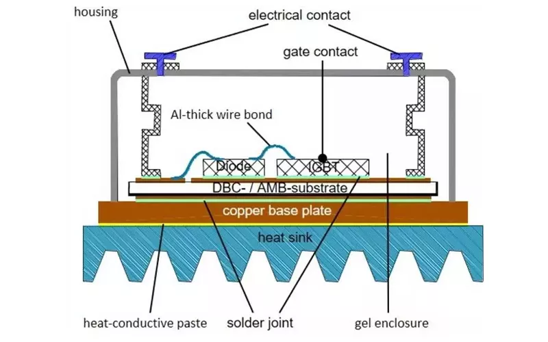
The figure above shows the typical location of a ceramic substrate and its function in a power electronic circuit. The ceramic substrate is usually found within the layers of copper or any other metal used.
Why are Ceramic Materials Used as Substrates?
Ceramic materials are used as substrates for three major reasons:
-
A Classified High-Performance Material
Ceramic substrates are an ideal replacement for fiber-reinforced epoxy (FR-4), where durability and performance are paramount. The latter material has favorable properties for a general-purpose PCB. However, ceramic substrates have unique and superior characteristics for high-tech PCBs, like impeccable mechanical stability and high temperature rigidity.
-
Универсальность
Ceramic substrates’ properties are applied in power electronics, multi-chip modules, hybrid microelectronics, and electronic packaging.
-
Emissions Control
The material maintains mechanical and structural integrity in harsh engine exhaust conditions. Besides, its lightweight nature and large surface area provide perfect conditions for catalytic processes.
“The substrate in flexible electronic devices is a bit like the foundation in your house. If it’s cracked, it compromises the mechanical integrity of the entire device.” – Nitin Padture, professor of engineering, Brown University.
Ceramic Vs. Polymer Substrates
Источник: Unsplash.com
Ceramic substrates are considered the best materials for high-performance applications like aerospace and automotive. Their polymer counterparts are used more for general-purpose PCBs.
Here are the key differences between ceramic and polymer substrates:
|
Свойство |
Керамическая подложка |
Polymer Substrate |
|
Теплопроводность |
Up to 200 W/(m.K) |
0.1 to 0.5 W/(m·K) |
|
Диэлектрическая проницаемость |
Up to 29 @1MHz |
2.1-3.4 ε |
|
Плотность |
Up to 6.0 g/cm³ |
Up to 1.4 g/cm³ |
|
Mechanics |
Durable |
Not durable |
|
Manufacturing process |
Complex |
Simple |
|
Расходы |
Дорогой |
Экономически эффективно |
|
Environmental effects |
Safe |
Not safe |
Examples of Ceramic Materials Used as Substrates
Ceramic materials are non-metallic, which is part of the reason why they are preferred. This demonstrates their excellent heat dissipation and reliability.
Here are the most common ceramic materials used as substrates in the market:
-
Нитрид алюминия (AlN)
-
Глинозем (Al2O3)
-
Нитрид кремния (Si₃N₄)
-
карбид кремния (SiC)
-
Цирконий (ZrO₂)
-
Оксид бериллия (BeO)
Find more information about each ceramic material’s properties that support its use as a substrate здесь.
Ceramic Substrate Manufacture
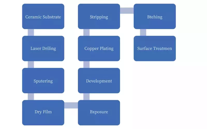
The above chart shows a typical manufacturing process of ceramic substrates.
In simple terms, ceramic substrate manufacture can be broken down into three steps. The substrate creation, the connection layer, and the circuit layer.
As we said earlier, the ceramic substrate acts as a base or a foundational support. You get the electrical interconnections in the connection layer. The final layer contains the printed circuit that facilitates the performance of the electronic device.
HTTC (High-Temperature Co-Fired Ceramic) is the most popular manufacturing process. It takes the following steps:
-
Спекание: The manufacturer creates a solid ceramic by mixing powders without glass. The mixture is then sintered at temperatures as high as 1,600°C
-
Drilling: This happens if through-holes are required. Hence, the manufacturer drills the substrates at high temperatures
-
Metal paste printing: Metallic powders are mixed with binders to create a paste. The manufacturer then applies the paste on the substrate to create the circuit layer
-
Sintering aid addition: You add 4-8% of sintering aid to facilitate sintering
-
Layer lamination: Happens depending on the component design and the number of layers
-
Final sintering: Temperatures are as high as 1650°C, allowing the layers to solidify. It also completes the circuit board.
-
Soldering: A solder mask is applied to the circuit board to provide protection
Other widely used options include Direct Bonded Copper (DBC) [1] and Thick Film Ceramic PCB [2].
Industrial Relevance of Ceramic Substrates
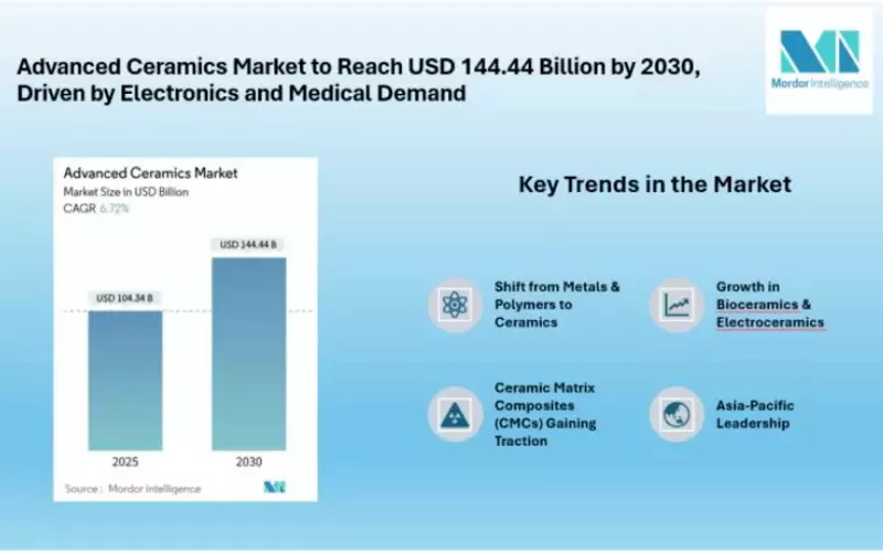
Источник: Mordor Intelligence
The above market analysis projects the global ceramic substrate market will exceed USD 144 billion by 2030, growing at a 6.42% CAGR. Its end users’ diverse needs play a key role in the growth of its market.
According to the study by Mordor Intelligence, the ceramic substrates market is gaining traction due to the widespread migration from metal and polymer substrates to ceramics.
Recent developments have led to significant growth in both bioceramics and electroceramics.
In bioceramics, demand for biocompatible components is projected to grow at an above-average rate of 11.84% CAGR.
Likewise, electroceramic components play a critical role in the medical field. Their market share was almost half the total global market size. The size is expected to grow steadily as the demand for such components is bound to increase.
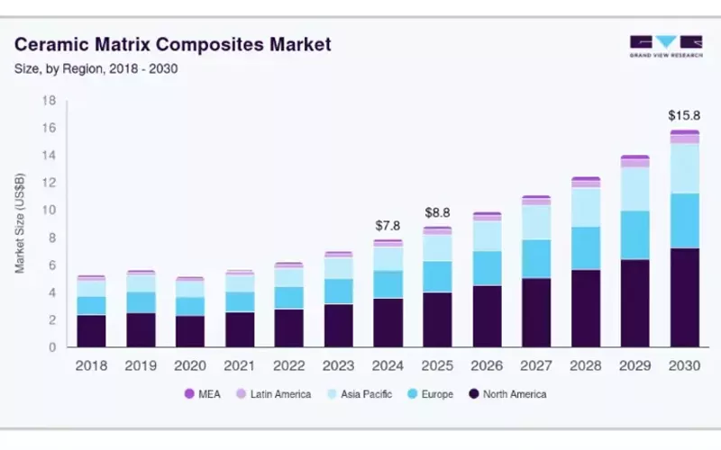
Источник: Grand Review Research
Ceramic matrix composites enhance the fracture toughness of traditional ceramic substrates. According to the above chart, CMCs are expected to hold a USD 15.83 billion market share by 2030.
The composites’ characteristics, like low weight, high temperature endurance, and durability, are ideal for missile use, aircraft components, and thermal protection applications.

Источник: Unsplash.com
Renewable energy systems and industrial gas turbines also help grow the CMC market size due to the recent global emphasis on clean energy.
Industries see CMCs as a crucial material in modern energy solutions for their reduced maintenance costs, operational efficiency, and rigidity in extreme conditions.
“The additive manufacturing of composite structures can open possibilities in the design and fabrication of devices but also demands new approaches.” – Luliia Tirichenko, Doctor of Philosophy, Imperial College London
|
Segmentation |
Sub-segment Type |
Sub-segment with High Growth Projectory |
|
Ceramic substrate types |
Aluminium nitride, alumina, beryllium oxide, silicon nitride |
Aluminium nitride |
|
Form |
Plates, sheets, film |
Ceramic plate |
|
End-user market |
Consumer electronics, military, spacecraft electronics, automotive, telecom |
Consumer electronics |
|
Region |
Asia-Pacific, North America, Europe, Rest of the World |
Asia-Pacific, followed by North America |
FAQ About Ceramic Substrates
1. Why is There a Global Shift to Ceramic Substrates?
Ceramic substrates are an interesting, robust material with a unique combination of properties. They are thermal resistant, lightweight, durable, environmentally friendly, and are actively being developed to be cost-effective. Hence, they are ideal for diverse industry applications.
2. How are CMCs Related to Ceramic Substrates?
CMC-ы enhance the fracture toughness of traditional ceramic substrates. Ceramic fibers are embedded within a ceramic matrix, giving a more rigid composite material.
3. Why Are CMCs So Much Used in Avionics?
Ceramic matrix composites are adopted in aerospace electronics because they promote fuel efficiency. Their low weight and thermal stability make them ideal for aircraft engines.
4. Which is the Biggest Challenge Investors in Ceramic Substrates Face?
Investors face high production costs – expensive raw materials and complicated manufacturing processes. However, automation and supply chain integration help improve the situation.
5. How are Researchers Solving the High Production Cost Problem?
Research entities are proactively involved in enhancing CMC properties and introducing cost-effective production techniques. Such techniques include hybrid CMC processing and additive manufacturing, furthering their deployment in different economic sectors.
6. Why is the Asia-Pacific Region the Largest Market for Ceramic Substrates?
The Asia-Pacific region has the largest ceramic substrate market because investors are mainly focusing on energy infrastructure, semiconductors, and medical devices. These heavily increase the demand for ceramic substrate materials. Government incentives also further this market growth.
Get Started Today!
Великолепный is an authentic and reliable company specializing in advanced ceramics. Besides legit ceramics, we facilitate a transparent onboarding process with supportive customer service. So, you don’t have to be stranded, undecided on what to choose!
Click здесь поговорить с нами сегодня!